The ‘dual_sided_component’ property in the Allegro PCB Editor 16.6 release can be leveraged to support vertical component applications. Apply the property ‘dual_sided_component’ to the symbol definition. Assuming a two-pin component, you will map pin 1 and pin 2 to unique padstacks, each with a ‘Begin’ or ‘End’ layer pad defined. The base layer is established using the Embedded Layer Setup form. The alternate layer pin is determined based on the value of the package height and stackup construction: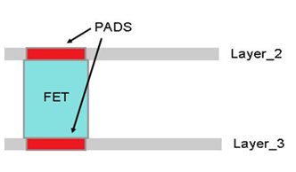
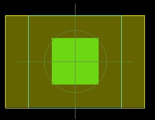
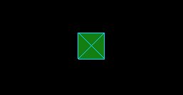
I’ll explain this capability using an example. Consider the following symbol comprised of two coincidently placed pins, assembly outline and place bound shape:
a. Pin 1 is mapped to padstack 20x20t (BEGIN layer pad defined)
b. Pin 2 is mapped to padstack 20x20b (END layer pad defined)
c. The ‘Package_Height_max’ property is set to 38 mils
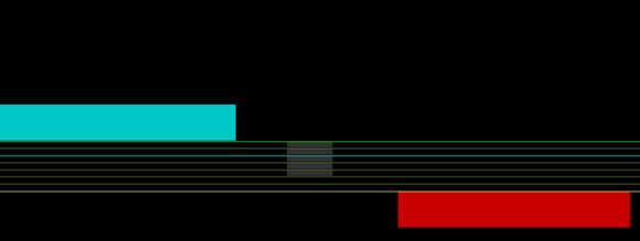
The two pad files (20x20t.pad and 20x20b.pad) are displayed below:
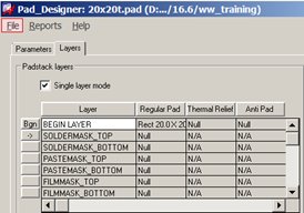
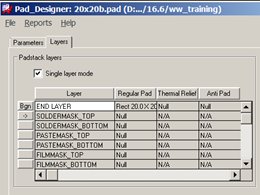
Begin Layer End Layer
Open ‘Embedded Layer Setup’ form - Setup – Embedded Layer Setup from a .brd file. As an example, for SIGNAL_6 – Change ‘Embedded Status’ to ‘Body up’ and ‘Attach method’ to ‘Direct Attach’:
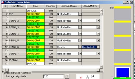
Place one Cap then note the DRC ‘C-H’. This indicates the height of the Cap package is greater than the dielectric thickness between layers SIGNAL_5 and SIGNAL_6. Based on the height of the Cap and stackup construction, the ‘alternate’ pad for the Cap appears on layer ‘Top’.
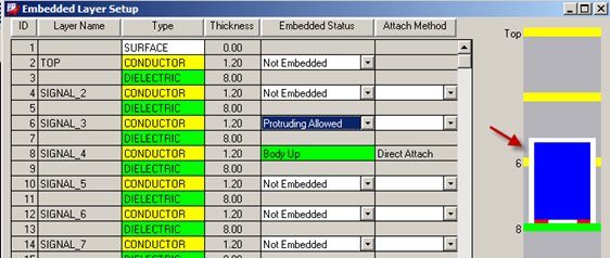
Open the ‘Embedded Layer setup’ form once again and change ‘Embedded Status’ to ‘Protruding allowed’ for SIGNAL_2 through SIGNAL_5. This will permit the Cap to pass through all these layers:
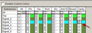
Enable the visibility of the Cavity Subclass associated with SIGNAL_3:
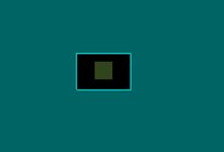
Confirm the ‘alternate’ pad of the vertical component is associated with layer ‘Top’:
Review the design in 3-D (enable the visibility of all layers and placebound shapes):
Please share your observations of this new capability.
Jerry “GenPart” Grzenia