Quantcast
Channel: Cadence PCB Design Blogs
Viewing all 668 articles
Browse latest View live

What's Good About Capture’s Design Rule Checks? 16.6 Has Several New Enhancements!

$
0
0

The Allegro Design Entry CIS (OrCAD Capture) 16.6 release provides extensions to the Design Rule Checks (DRC) system. The Custom DRC provides the ability to extend the Capture DRC system to user-defined rules.

Open an Allegro Design Entry CIS design database (.dsn) file, select a design in Project Manager, and click menu Tools > Design Rules Check:


Click on Configure Custom DRC:


The following DRCs are provided as examples:

  • Hanging Wires
  • Device Pin Mismatch
  • Overlapping Wires
  • Reference Prefix Mismatch
  • Port-Pin Mismatch
  • Shorted Discrete Part

Enable all DRCs to execute, select the checkbox “Run Custom DRC”, and then select OK to execute DRC. Here’s an example output:

All TCL code for the DRCs above is available in <$CDSROOT>\tools\capture\tclscripts\capDRC.

In the schematic, you can select any DRC and use RMB Waive DRC:


The DRC is added to the Waived DRC list and does not show on the schematic canvas anymore.

In the DRC form, you can use the Selection Filter for a group of DRCs: Use Menu View > Selection Filter followed by clearing all checkboxes except “Markers”. Select a group of DRCs and waive them. Rerun DRC with “Preserve Waived DRC” checked:


All waived DRCs remain hidden. Use Select Filter to un-waive a group of DRCs in an area. Use RMB > UnWaive DRC. Now run DRC again with the checkbox cleared for “Preserve Waived DRC”—all DRCs should reappear.

As always, I look forward to your feedback!

Jerry “GenPart” Grzenia


What's Good About Allegro PCB Editor Dual-Side Contact Components? It’s in the 16.6 Release!

$
0
0
The use of dual-sided contact components when placed on internal layers of the PCB allows connections to be made from either side of the device. One of the benefits of using this emerging technology is the reduction of core vias that may have been used to make connections from the component to either side of the PCB. Symbols targeted for dual-side applications must have the property ‘dual_sided_component’ applied in the Allegro Symbol Editor. The associated padstacks of the symbol must have a ‘begin’ and ‘end’ layer pad defined.

When the symbol with the dual-sided property is placed, the ‘begin’ pad defined in the padstack definition is mapped to the inner layer upon which the component is placed. The alternate pad, defined as the ‘end’ pad at the definition level, is mapped to the layer closest to the top of the component based on the component height.

Existing Allegro embedded setup methodologies are fully supported; direct or indirect attach as well as body up/down. Since the stackup is unlikely to be constructed with material thickness that aligns with the component height, it’s likely the indirect attach method is used for this technology. 


Read on for more details …

There are two prerequisites required at the symbol definition level -
1. Add the property ‘dual_sided_component’ to the symbol definition
2. The associative padstack must have a ‘BEGIN’ and ‘END’ pad defined


The property assignment must be made in the ‘Symbol Editor’, not the ‘PCB Editor’. When in the ‘Symbol Editor’, the property is applied to the ‘drawing’ as shown below:


As an example, consider changing the embedded layer setup (using the Setup > Embedded layer setup form) for SIGNAL_4 to the values specified below for “Embedded Status” and “Attach Method”:


In the “Placement Application mode” Options Panel you should see components in the placement list. The letter ‘E’ indicates the component has been assigned the ‘Embedded_Placement’ property and the green background indicates the property value is set to ‘Required’:


When you place the components, you’ll note the following -
  • You will not be allowed to place these components on the outer layers as a result of the components having the ‘dual_sided_component’ property applied
  • When initially moving any of the resistors from the placement list, they will automatically drop to the embedded layer (SIGNAL_4). There is no RMB action necessary when the component has a ‘required’ property value and there is only one embedded layer identified in the stackup.
  • The component pads are suppressed when using ‘Indirect Attach’ method
  • You should see 2 indirect symbol vias on SIGNAL_4


Disable the visibility of layer Signal_4, The alternate side of the component is based on its symbol height value. Based on the height of the symbol and thickness of the dielectric, via pads in this case will appear on SIGNAL 3:


Invoke ‘Add Connect’ then adjust option in panel to ‘WL’ (Working Layer):


Use the ‘3-D viewer’ to display your routed design. Enable the visibility of the place-bound shapes for all subclasses (top, bottom, embedded):


Please share your experiences using this capability.

Jerry “GenPart” Grzenia

What's Good About Allegro PCB Editor Multiple Constraint Region Assignments? 16.6 Has It!

$
0
0

Just a short post today.

In the 16.6 Allegro PCB Editor release, multiple region shapes can now be assigned to a single region constraint object. Using the General Edit Application mode, pre-select multiple region shapes, then use the context-sensitive RMB menu to access the Assign to Region command.

Ensure you are in General Edit Application mode. Consider an example where we will assign the region shapes associated with the components U7 and U8 to a "BGA" region constraint object.

Window-select the two purple region shapes, or hold down the CONTROL key, then select each shape individually. Hover over any one region shape, then RMB—Assign to Region. Select "BGA" from the list:


I look forward to your comments!

Jerry “GenPart” Grzenia

What's Good About Allegro DEHDL Net Renaming? The Secret's in the 16.6 Release!

$
0
0
Just a brief post this week to mention a new capability for Allegro Design Entry HDL (DEHDL) that was made available in the 16.6-QIR4 release.

You can now employ net renaming without loss of data:
  • All instances of the net will be renamed to a new name
  • All properties and constraints captured on the net instances retained
  • All membership to net objects are retained

The net rename capability is available as:

  • A menu command
  • A context (RMB) menu command
  • Change of a net name
  • Using the Attribute Editor
  • Using the Change command
  • As a DEHDL console command:

    _netrename <old_net_name> <new_net_name>


I look forward to your feedback on this capability.

Jerry “GenPart” Grzenia

DDR4 Power-Aware Signal Integrity Adopting Serial Link Simulation Techniques

$
0
0

The signal integrity (SI) prophets had predicted this time would come, and it turns out they were right. The techniques that SI engineers have been using for the past decade to analyze multi-gigabit serial link interfaces are now starting to be applied to parallel memory interfaces, such as DDR4. And it all makes sense.

Back when PCI Express initially came out at 2.5Gbps, we saw a seismic shift in how simulation and analysis would be done, forever changing the SI landscape. The requirement to evaluate eye diagrams derived from huge bit streams of 10,000 bits or more pushed traditional circuit simulation into a characterization role, and convolution-based channel simulators came on the scene to handle the new high-capacity simulation needs. The need to efficiently model equalization effects, including real-time adaptation, gave rise to executable "algorithmic" models, and a new capability called "AMI" for "Algorithmic Modeling Interface" was driven into the industry-standard IBIS specification. Those were exciting times in the SI world, and Cadence was out in front leading the pack (see Interrogating the chips in this 2007 EE Times article).

Serial link analysis techniques such as bit error rate (BER) with bathtub curves, high-capacity simulation, and eye diagrams are now part of memory interface analysis.

Watch demo now


Now we have fast-forwarded  into a new era, and the memory interfaces we are dealing with today are looking eerily "serial linkish". The data rates we see for DDR4 data buses today are right where we were initially for PCI Express. DDR4 I/O structures are similar to what we have historically had in the SerDes space, with built-in pullup termination on-die, and nicely linear, symmetric, well-behaved output impedances. While signaling is still single-ended, data buses have moved closer towards point-to-point topologies, with more use of "clamshell" component placement on top and bottom of the PCB to cluster loads at the end of the transmission line when possible. And while equalization has still eluded off-the-shelf memory devices (largely for cost reasons), on the controller side of the interface we are seeing feed-forward equalization (FFE, i.e. pre/de-emphasis) becoming more and more common.

In addition to taking on serial link characteristics, the techniques used to analyze DDR4 are also shifting towards those traditionally used in serial links. Data bus compliance and timing for DDR4 has shifted from traditional cycle-by-cycle setup and hold criteria to a mask-based compliance, as commonly used with SerDes devices and serial links. Also, DDR4 JEDEC specs now specify a target BER; "The design specification is BER <1e-16 ... BER will be characterized and extrapolated if necessary using a dual dirac method ..." These are exactly the same types of specifications that serial link interfaces have been using for years.

So where does all of this lead us? Cadence Sigrity SystemSI - Parallel Bus Analysis has integrated the serial link channel simulation engine in, and successfully applied it to coupled, single-ended parallel buses, even including non-ideal power effects (patent pending). What does this bring us? First, it brings us simulation capacity, so you now have the unique ability to run hundreds of thousands or even millions of bits of traffic through the memory interface, way beyond the capacity of traditional circuit simulation. This lets you see what the eye is really going to look like in the lab, when you are sampling many, many bits worth of data on your oscilloscope. This also enables deterministic and random jitter to be injected, so you can see what effect that will have on the eye.

AMI modeling comes along for the ride as well. Once channel simulation is introduced, you are also free to use AMI models for the equalization used at the controller. FFE modeling used with serial link applications can be directly leveraged for controller equalization, and comprehensive AMI models are included with Sigrity SystemSI.

But fundamentally what all this simulation capacity and modeling enables is generation of a very detailed eye distribution, from which (with dual dirac statistical post-processing) bathtub curves can be produced, just like with serial links. The bathtub curves provide the key insight into the BER performance of the interface, which at the end of the day is what you really need to know as an engineer, whether you are working on parallel memory interfaces or serial links.

Grab a cup of coffee and watch the demonstration of our complete solution that uses channel simulation to perform BER analysis on DDR4 interfaces with Cadence Sigrity SystemSI - Parallel Bus. If you come from the SerDes space, a lot of this will look familiar to you, just as those new DDR4 specs probably do. But hey, as they say, what's old is new again. And just like before, Cadence is out in front.  As a wise man once said, unless you're the lead dog of the sled team, the view doesn't change much.  


Tell us about your experiences using SystemSI and Cadence Sigrity modeling and extraction technology.


Team Allegro 

What's Good About Allegro Design Workbench Team Collaboration? Find Out in the 16.6 Release

$
0
0

The Allegro Design Workbench Team Design Option (TDO) offers two (2) specific integrator roles for team design and collaboration:
Logical design integrator
  Responsible for front-end design
Physical design integrator
  Responsible for back-end design

A logical design integrator or physical design integrator needs to enable Team Design and assign and inform team members to work on the design project from the list of designers.

Read on for more details…


Logical design integrator (LDI)


The LDI has complete permission on logical objects as defined in the design and assigns users to logical objects of the design. The physical objects are shown as read only for an LDI and by default the LDI sees the logical hierarchy. The Team Design interface displays the schematic design in a hierarchical form. It shows all the blocks and its logical objects such as:
Schematic
Symbol
Package


Physical design integrator (PDI)


The PDI has complete permission on physical objects as defined in the design and assigns users to physical objects of the design. The logical objects are shown as read-only for a PDI and by default the PDI sees the Physical Hierarchy. The Team Design interface displays the physical design in a parent/child hierarchical relationship.  It shows all the blocks and:
Physical view
Collections
Partitions
Modules
Package view


TDO User Model

A team of users is assigned for ECAD projects - the users are assigned either using LDAP or the template file. The user doing ETD is either the LDI or PDI or both, based upon either the LDAP or the template file. All project users get read-only permissions on a design. Users working on particular design objects get read and write permissions on design objects within a project based upon user assignment.

TDO pulls out user IDs from the corporate LDAP system, and the LDAP query and filter are controlled using the ldap.config file under cdssetup.

When the teamassignmnettemplate.xml file is placed in the proper directory, and the environment variable is defined, the project team assignment phase will access the team assignment template, providing a list of the user IDs defined within the template.


What do you think about this capability?
Jerry “GenPart” Grzenia

Create Ideal Solder Mask Openings Around Bond Fingers with Cadence 16.6 IC Packaging Tools

$
0
0

Normal 0 false false false EN-US X-NONE X-NONE

Exposing metal through solder mask openings is as necessary as it can be frustrating. For regular arrays and grids of pins of a flip chip, embedding the openings directly in the padstack definition for the bumps is perfect. But, what about for wire bond designs?

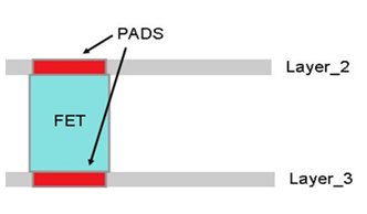
Fingers and power/ground rings need to be exposed so they can be bonded to, but visibility of surrounding metal should be minimized. At the same time, it is important that the openings themselves not have sharp corners which could cause manufacturing concerns like the mask getting peeled back.

As a result, it is not appropriate to use the solder mask pads in the finger pad definitions (which wouldn't help with the rings, regardless!). Instead, a smooth mask outline around sets of fingers in close proximity is the best approach.

How, then, do you go about making this happen? With the Cadence APD and SiP Layout tools in 16.6, the answer is the bond finger solder masking tool. Keep reading to learn more about what this handy tool allows you to do.

Creating Clean Solder Mask Openings

Near the end of your initial design of a substrate for a package with one or more wire bonded dies, it comes time to define the solder mask openings. APD and SiP Layout provide you with a tool specifically to accomplish this task. You can find it under the Manufacture -> Create Bond Finger Solder Mask menu item. 

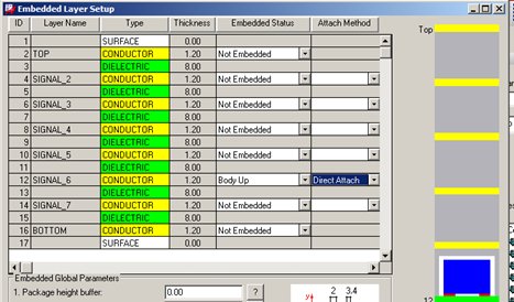
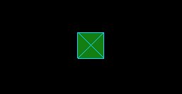
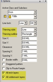
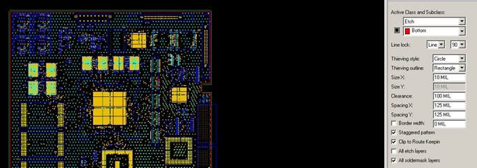
With a simple interface (see for yourself, below!), you get all the controls that you need. There are two modes to give you the flexibility you need, with different options for bond finger exposure and power/ground ring openings. 


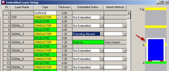
When creating mask openings for fingers, you should take special note of the field at the very bottom. By controlling the intent width, you can eliminate any potentially sharp corners on the inside of the mask shape between fingers. This way, you get a smooth, clean opening around an entire tier of fingers with one simple selection.

Conversely, for bonds to your rings, you can expose only the pieces of the ring which have bonds to them. The mask openings can even be trimmed to the edge of the shape to make sure no nearby clines are accidentally exposed.

Do you have a need to create these types of masks around a set of vias on your substrate layer? Do you have some pins, perhaps, where using the padstack-embedded solder mask pad shape is not suitable? Fret not. Turn on the "icp_soldermask_allow_pins" option in your User Preferences editor and you can define masks for these objects with the same settings you have when masking traditional fingers. How's that for flexibility?

What If I Need to Move My Bond Fingers After I've Generated My Shapes?

Fear not! ECO and design revisions are a fact of life. When you receive an order that requires changes to the bond finger pattern, you can make those changes knowing that, when complete, the mask openings can be quickly and easily updated.

Using the same manufacturing command, make sure that you have the "Delete existing solder mask" option enabled at the top of the options (it is on in the screen shot above). This will automatically delete the old shapes as you select the fingers you have moved or added, leaving just the new mask. This ensures that you don't have overlapping masks that could result in undesirable outlines or - even worse - the exposure of clines and vias that are where one or more of the old fingers used to be.

What Tools Are Available for Validating My Solder Masks Are Correct?

Once you have your solder masks defined (or after updating them because of a design change request), it is important to validate that only the right objects are going to be exposed during manufacturing of your substrate.

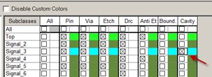
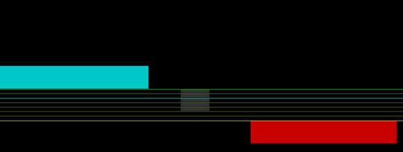
The APD and SiP Layout tools provide you with a number of checks beyond the basic solder mask online DRCs. You can configure these under the Assembly worksheet in Constraint Manager and run them from the Manufacture -> Assembly Rules Checker... command, shown below with the 16.6 solder mask rules:


If you want to write your own checks, you can use the RAVEL tool to define custom rules. Or, for pure 
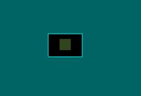
visualization of the metal exposed by the solder mask shapes (particularly useful for documentation purposes), you can use the layer compare tool set, which we covered in an earlier entry in this series. By doing a logical AND between the solder mask layer and the corresponding substrate conductor layer, you can create a layer showing only the metal that is visible through holes in the solder mask. There's even the option of viewing things in the 3D Viewer, where you can see the bond wires and their clearance from the masks as they get close to the substrate! Talk about choices!

How Do You Define Your Solder Masks?

Armed with these tools, are you eager to make your design flow more efficient? If you have an idea for how to make these tools even more powerful, we would love to hear it. Give your Cadence support representative a call and let us know your ideas. Just don't be surprised if, with the next software release, you see your idea realized in the tool!


Jeff Gallagher

/* Style Definitions */ table.MsoNormalTable {mso-style-name:"Table Normal"; mso-tstyle-rowband-size:0; mso-tstyle-colband-size:0; mso-style-noshow:yes; mso-style-priority:99; mso-style-qformat:yes; mso-style-parent:""; mso-padding-alt:0in 5.4pt 0in 5.4pt; mso-para-margin-top:0in; mso-para-margin-right:0in; mso-para-margin-bottom:10.0pt; mso-para-margin-left:0in; line-height:115%; mso-pagination:widow-orphan; font-size:11.0pt; font-family:"Calibri","sans-serif"; mso-ascii-font-family:Calibri; mso-ascii-theme-font:minor-latin; mso-fareast-font-family:"Times New Roman"; mso-fareast-theme-font:minor-fareast; mso-hansi-font-family:Calibri; mso-hansi-theme-font:minor-latin; mso-bidi-font-family:"Times New Roman"; mso-bidi-theme-font:minor-bidi;} 

Customer Support Recommended – Using Test Points in Allegro Design Entry CIS and Allegro PCB Editor Flow

$
0
0

test point is a location within an electronic circuit that is used to either monitor the state of the circuitry or to inject test signals. Test points have two primary uses:

  • During manufacturing they are used to verify that a newly assembled device is working correctly. Any equipment that fails this testing is either discarded or sent for rework.
  • After sale of the device to a customer, test points may be used at a later time to repair the device if it malfunctions, or if the device needs to be re-calibrated after having components replaced

A test point can be a simple pad on a net, a through hole, or a pin where test equipment can be connected. Figure 1 shows a test point on a via.

Figure 1 - Test point on a via

The application note discussed here helps you understand the test point flow from OrCAD® Capture to Allegro® PCB Editor and vice versa. This document explains different ways of defining test points in OrCAD Capture and transferring these to Allegro PCB Editor. The application note also explains how to identify nets on which a test point is to be defined in Allegro PCB Editor.

Defining Test Points

Test points are used in PCB boards for testing signal continuity. They are added in the PCB board itself to verify the circuit or to provide test input signals. Allegro PCB Editor allows defining test points on nets, vias, and pins. However, in recent times, it has been observed that schematic engineers have expressed the need of defining test points in the front-end schematic itself. Owing to their knowledge of circuit and critical signals/nets in the design, schematic engineers wish to identify the net on which test points should be added on the PCB board.

This document discusses how you can define test points on nets in the schematic. You can take either of the following two approaches:

  •   Identify the nets on which a test point is to be added
  •   Filter off the nets on which test points are not added, allowing Allegro PCB Editor to choose all other nets for Testprep. This is done by defining the NO_TEST property.

Defining Test Points in Allegro PCB Editor

In Allegro PCB Editor you can define test points directly even if it is not defined in the schematics. A test point is generated in Allegro PCB Editor using Testprep. Testprep adds test points on nets which do not have NO_TEST property defined on them.

In Allegro PCB Editor, while using Testprep you can assign the following properties:

  • NO_TEST: Attach to nets that do not require test points. In Allegro Constraint Manager, this property is specified as Prohibit.
  • TESTPOINT_QUANTITY: You can limit the number of test points that will automatically be added to the net using this property.

The two properties, NO_TEST and TESTPOINT_QUANTITY, are displayed in Allegro Constraint Manager as shown in Figure 2.


Figure 2 - Allegro Constraint Manager showing test point properties

Refer to the following document for details on running Testprep:

http://support.cadence.com/wps/mypoc/cos?uri=deeplinkmin:DocumentViewer;src=dt;q=cspb_board_design/testpoint.pdf

Defining Test Points in Schematic

You can either directly define test points on nets in the schematic or identify the nets on which test points are to be added in Allegro PCB Editor.
The following sections explain the different methods of defining test points in schematic.

By adding a single pin component

Place a single pin component on the net in the schematic design on which the test point is to be defined. This single pin component can itself be treated as a test point in Allegro PCB Editor.
The footprint (PCB Editor Symbol) of this component can be a pad which will be placed on the net and work as a testpoint.

Figure 3 - Single pin component used as a test point

In the example test case, the TP_SinglePinComponent directory has a schematic and its board file, which uses a single pin component as a test point. A sample single pin component and its footprint (pad) are also present in it.

By adding property ‘NO_TEST'

As discussed above, Testprep adds test points on nets which do not have NO_TEST property defined on it.

You can identify nets on which a test point is not to be added by defining the NO_TEST property on the nets in the schematic design. To add NO_TEST in Capture, select the nets, open property editor, and click New Property to add a property with the following details:

NAME=NO_TEST

Value=YES

NO_TEST defined in schematic is transferred to Allegro PCB Editor as a net property. You can also add or delete this property from nets in Allegro PCB Editor.

Backannotating Test Point Properties to Schematic

The board designer can define or modify the NO_TEST property directly on board in Allegro PCB Editor before running Testprep to add testpoints. This information is transferred to the schematic through back annotation.


As discussed in Defining Test Points in Allegro PCB Editor , while using Testprep you can assign the following properties in Allegro PCB Editor:

  • NO_TEST
  • TESTPOINT_QUANTITY
  • TESTPOINT_ALLOW_UNDER
  • TESTPOINT_MAX_DENSITY

Among these properties, NO_TEST and TESTPOINT_QUANTITY are defined on nets and can be back annotated to the schematic. For this, make sure that the properties are set to YES in the allegro.cfg file under the [netprops] section.

TESTPOINT_ALLOW_UNDER and TESTPOINT_MAX_DENSITY cannot be back annotated to the schematic as these are defined on symbols in Allegro PCB Editor.


Refer to the app note here for the detailed step-by-step procedures on the complete flow, including a test case attached to the app note.

Note: The above link can only be accessed by Cadence customers who have valid login credentials for Cadence Online Support (http://support.cadence.com).

Naveen Konchada
Cadence Customer Support


What's Good About Capture’s Design Rule Checks? 16.6 Has Several New Enhancements!

$
0
0

The Allegro Design Entry CIS (OrCAD Capture) 16.6 release provides extensions to the Design Rule Checks (DRC) system. The Custom DRC provides the ability to extend the Capture DRC system to user-defined rules.

Open an Allegro Design Entry CIS design database (.dsn) file, select a design in Project Manager, and click menu Tools > Design Rules Check:


Click on Configure Custom DRC:


The following DRCs are provided as examples:

  • Hanging Wires
  • Device Pin Mismatch
  • Overlapping Wires
  • Reference Prefix Mismatch
  • Port-Pin Mismatch
  • Shorted Discrete Part

Enable all DRCs to execute, select the checkbox “Run Custom DRC”, and then select OK to execute DRC. Here’s an example output:

All TCL code for the DRCs above is available in <$CDSROOT>\tools\capture\tclscripts\capDRC.

In the schematic, you can select any DRC and use RMB Waive DRC:


The DRC is added to the Waived DRC list and does not show on the schematic canvas anymore.

In the DRC form, you can use the Selection Filter for a group of DRCs: Use Menu View > Selection Filter followed by clearing all checkboxes except “Markers”. Select a group of DRCs and waive them. Rerun DRC with “Preserve Waived DRC” checked:


All waived DRCs remain hidden. Use Select Filter to un-waive a group of DRCs in an area. Use RMB > UnWaive DRC. Now run DRC again with the checkbox cleared for “Preserve Waived DRC”—all DRCs should reappear.

As always, I look forward to your feedback!

Jerry “GenPart” Grzenia

What's Good About Allegro PCB Editor Move Lines/Text to Different Classes? Check Out 16.6!

$
0
0

Beginning with the 16.6 Allegro PCB Editor release, lines and text can now be moved outside their present Class-Subclass structure. In previous releases, workarounds using the clipboard were necessary to accomplish this task.

Hover over the line, text, or rectangular element, then use the RMB to access the "Change Class/Subclass" command. Select a new class, then one of the subclasses within the Class structure from the popup dialog.  

Select General Edit Application Mode and hover over different elements (text, line, unfilled rectangle) in an Allegro PCB Editor .brd file, then use the RMB to access the "Change Class/Subclass" command. Move the elements to a new Class-Subclass; Drawing Format – Outline for example:


Snap Updates

The "Snap Pick to" command has been enhanced with the following RMB options:

  • Rectangle Edge Vertex
  • Rectangle Edge Midpoint
  • Rectangle Edge
  • Shape Center
  • Symbol Center

In addition to the new options, the "Edit-Vertex" command is now integrated with the snap function.


Some Examples
Add a leader line from the midpoint of a rectangle side. Select Manufacture – Dimension Environment – RMB – Leader Line and hover over a side segment, then use RMB – Snap Pick to – Rectangle Edge Midpoint:

Add a line to the corner of the rectangle. Add – Line. Set "Line Lock" to "Off". Begin the line in black space and end near the corner of the rectangle using RMB – Snap pick to – Rectangle Edge Vertex:


Add line to a user-selected location on a rectangle edge. Add – Line. Begin the line in black space and hover over the rectangle edge then RMB – Snap Pick to – Rectangle Edge:


I look forward to your comments.

Jerry “GenPart” Grzenia

What's Good About Allegro PCB Editor New Slide Capabilities? 16.6 has Several New Enhancements!

$
0
0

The 16.6 Allegro PCB Editor release's new ‘Slide’ command utilizes a move-intersect algorithm that delivers smoother, more predictable, and localized edits. This change has allowed for simplifying the use model, integrating sliding of off-angle and arc routing, and providing new options to improve efficiency. In 16.6, the standard ‘Slide’ command has been replaced with a new version and is accessible in the same way as previous Allegro methods to invoke ‘Slide’. The following options are available while running the ‘Slide’ command:


New Slide Options:

  • Min Corner Size: A fill-in field for minimum 45-degree corner size allowed between two non-parallel cline segments.This field also supports ‘[N] x width’ values.   
  • Min Arc Radius: A fill-in field for minimum arc size allowed between two cline segments. This field also supports ‘[N] x width’ values. This value prevents arcs from completely collapsing during slide operations.
  • Vertex Action:  A drop-down field that controls what action occurs if the user selects at vertex between two segments during Slide. A special vertex cursor is shown to the user as an indication when a pick will get the vertex rather than a segment. The available actions are:
    • Line Corner – causes the current angle at the vertex to be split and a new segment is created. The new segment is then active on the cursor and can be modified with Slide. This would allow the user to change a 90-degree corner into a 45, or split any other existing angle. This is very useful to cleanup 90 corners, adjust off-angle corners, or reduce length of existing routes.
    • Arc Corner – causes an arc to be created at the selected vertex. The new arc is then active on the cursor and can be modified with Slide. This is very useful to convert 90 or 45 corners to arcs.
    • Move (default) – causes the vertex to ‘move’ as both adjacent segments are modified with Slide.   
    • None – prevents any special action when a vertex is selected.   
  • Auto Join: This option controls the behavior when parallel cline segments meet during a slide operation. The ON behavior of this option causes parallel cline segments to join as they meet during the slide operation, allowing the user to continue the current operation on larger sections of the cline. The OFF behavior of this option does not join parallel cline segments when they meet (unless a click is made), but instead creates new segments to connect the parallel cline segments.
    • Default Setting = On
    • Holding CTRL key during the slide operation will give the opposite behavior of the current setting on the Options form. This is useful to get the alternate behavior for Auto Join during a single edit, without having to switch the option setting.
  • Extend Selection: This option makes it easier for the user to preserve the connective pattern of multiple cline segments during a slide operation.  The ON behavior of this option extends the original selection made in the slide operation to include the two cline segments adjacent to the selection (additional segment on each side). The OFF behavior has no effect on the original selection.
    • Default Setting = Off  (it is recommended to use SHIFT for the ON behavior during specific slide operations)
    • Holding SHIFT key during the slide operation will give the opposite behavior of the current setting on the Options form. This is useful to get the alternate behavior for Extend Selection during a single edit, without having to switch the option setting.
    • This option is very efficient for sliding tuning patterns or other multi-segment structures when it is desired to keep the basic shape of the cline segments, without having to do a window selection on the segments.
    • Arc corners – Extend Selection can be used when sliding a 45-/90-degree segment that has arc corners, and the user wants to maintain the arcs while the selected segment slides (similar to previous “arcs with segments” option).


The following options have been removed:

  • Corners
  • Max 45 len
  • Add at max
  • Vias with segments
  • Ts with segments
  • Arcs with segments
  • The Enhanced Arc Editing mode has been removed as a RMB option. New Slide always runs in Enhanced Arc mode when arcs are involved in the slide operation.


Read on for more details …

Let’s first review the ‘old slide’ command as it related to the issue of ‘re-cornering’. Part of the challenges working with the ‘old slide’ command was corner management. Designers frequently adjust the ‘Max 45 len:’ parameter to either a big (99999) or little (10) corner sizes. Often the parameter is the opposite of what is required for a particular trace segment edit. For example - ‘Max 45 len’ set to 99999.00 expands a small corner (e.g. tuning):
     
     
Conversely when ‘Max 45 len’ is set to 10 or lower, sliding a segment with a long corner may result in the unfavorable condition where the corner is shortened, resulting in a cumulative effect on adjacent circuitry. Often, the modified circuit will be out of the Designer’s view screen:


Another common condition we see on designs is fracture trace runs. A pick on the highlight segment below would essentially split the trace into two district sections as shown in the second graphic:


Working with offset routing is becoming more popular and ‘Add Connect’  in 16.6 addresses those challenges; however, if we take a look at an old slide, here are some of the results:

 
With ‘Max 45 len’ set to 10 or 99999, we get this undesirable result:


So what does a user do? Corners must be set to ‘OFF’!  Not an obvious solution to the end user:
 .


How does one simply extend the trace segments represented by the arrows below?


Some of the results as I experimented with different settings:
     
                     
Best practices suggest windowing around the 3 segments, resulting in a ‘3 segment group slide’:


Let’s see how the new Slide command addresses these conditions. Invoke Etch Edit Application Mode. ‘Slide’ the segment as shown in the graphic below, noting the corners are adjusted, not regenerated, during the slide action. The tuning to the right is not destroyed:


Make single picks on any of the angled segments and note how new slide maintains the integrity of the routes:


Hover over what appears to be a contiguous line, noting it’s really comprised of 2 segments. ‘Slide’ the line noting the default ‘joining’ behavior: 

 
One of the new ‘Slide’ options is ‘Auto Join’. This option is enabled by default. Use the Control key during the action to toggle the behavior:


Use slide to join the segments into 1 contiguous one. Consider disabling the ‘Auto Join’ behavior to experience the old slide behavior. This may require you to ‘UNDO’ a few steps: 


Make picks as directed by the arrows in the graphic below, noting the initial behavior of slide. Now hold down the Shift key to toggle the option, ‘Extend Selection’. You are now performing a 3-segment slide operation:


Perform some of the same steps with the arc-based tuning:


There are 4 options related to vertex behavior when using slide: ‘Line Corner, Arc Corner, Move and None’:


Invoke ‘Slide’ then hover over the vertex location, noting the change in cursor display. With the option set to ‘Move’, select the vertex and note the 2-segment slide behavior:


Set the vertex option to ‘Line Corner’. Select the vertex again and note the trimming behavior. Select the Diff Pair vertex just above the GND net and perform the same action. This trimming technique can be used to reduce trace length to meet timing requirements:


Set the vertex option to ‘Arc corner’. Select the vertex points associated with the offset routing:

 
A method to convert the 45 corner to 90 is:
a.    Set ‘Min Corner Size’ to ‘0’
b.    Slide the corner until the angle becomes orthogonal:


Select the vertical segment while in the slide command, then press the Shift key to toggle the ‘Extend Selection’ option:


The Slide command is now ‘same net’ aware. Slide the vertical segment to left, noting the temporary DRC highlighting:

 
Perform a group slide on the 2 Diff Pairs and note the behavior associated with the diagonals:

       
Previously, the coupled segments would short to each other as outlined in the graphic below:


Improvements have been made to gather the Diff Pairs coming INTO the pads. The workaround for many users is to exit rather then enter pins during Diff Pair routing. Complete the route into the connector pins. Control the gathering of the Diff Pair by placing your cursor to the left or right side of the pad:


Please share your feedback using these new features.

Jerry “GenPart” Grzenia

What's Good About Allegro PCB Editor Artwork Film Capabilities? 16.6 Has Several New Enhancements!

$
0
0

The 16.6 Allegro PCB Editor release contains several enhancement to the Artwork Film generation.

Read on for more details …


Film Domain

Artwork films can now be designated by the domain where they appear. There are four domains available; Artwork, PDF, IPC2581, and Visibility. Access the User Interface by clicking on ‘Domain Selection’. One of the benefits of the domain form is the ability to segregate films for artwork versus films for PDF out:


Select Manufacture – Artwork, then click the ‘Film Control Tab’. Click the ‘Domain Selection’ Tab:


Artwork Film Name Update 


Film names have been increased from 17 to a maximum of 46 characters.


Artwork Option - Draw Holes


The film control form has been enhanced with a new option called ‘Draw Holes only’. The PIN and/or VIA CLASS must be specified for the film to control which holes are plotted. The option is not allowed if the film record includes ETCH Class. The holes that are plotted are true size; this includes oval or rectangular slots.

It’s probably best to disable the visibility of all layers - ‘Color Dialog – Global Visibility’ = ‘off’:


Select Manufacture – Artwork, then click the ‘Film Control Tab’. Delete the ETCH Class associated with the ‘Bottom’ Film record; use RMB – Cut:


Check the box adjacent to layer ‘Bottom’ and enable the ‘Draw Holes Only’ option, then click ‘Create Artwork’:


Import the artwork layer, File – Import – Artwork. Browse to the Bottom layer artwork file and select a class/subclass to which you want to import the data. Click ‘Load File’:


Place the bounding box anywhere in the workspace (here are the resulting artwork drill holes):


Please share your experiences using these new capabilities.

Jerry “GenPart” Grzenia

What's Good About Using Sigrity and Cadence SiP Digital to Reduce Design Costs? Check Out These Expert Insights Videos!

$
0
0

This week, you can view a couple of videos where customers describe how they used the Sigrity and Cadence SiP Digital Layout products to simulate, verify, and reduce the size and costs of their designs.

Ericsson Meets DDR and PCIe Specs While Avoiding Crosstalk
In this Expert Insights video from CDNLive India 2014, Sheetal Jain, a member of the modem organization at Ericsson Design, discusses how his team verified their design to meet DDR and PCI Express (PCIe) specs while avoiding crosstalk. They were able to simulate and verify using Cadence's Sigrity solution with the IBIS/AMI virtual reference design for interface compliance signoff, which they found to be easy to set up and easy to test, while saving them time and money. After watching this video, learn more about Cadence Sigrity SI/PI solutions.

(Please visit the site to view this video)


Reducing Cost, Size of PCBs with Embedded Technologies and Cadence Layout Tools
Dialog Semiconductor faced a potentially daunting challenge: reduce the size and cost of its PCBs via embedded passive devices at the substrate level. The company needed a tool that could help migrate from a two-layer BGA substrate to four layers. Rajesh Aiyandra, package design and simulation team leader at Dialog, explains how Cadence SiP Digital Layout helped deliver a smooth migration, from the change in the number of layers to the change in the via specifications. After watching this video, learn more about Cadence SiP Digital Layout.

(Please visit the site to view this video)

I hope you enjoy watching these!

Jerry "GenPart" Grzenia

Multi-Fabric Planning for Efficient PCB Design

$
0
0

Recently, an article was published in Printed Circuit Design and Fab about Multi-Fabric Planning for Efficient PCB Design(see page 22 of printed magazine).

Today's BGA-style packages have a significant impact on PCB layer count, route complexity, and cost. Efficient BGA net assignment and patterning of power and ground pins can make the difference between a four- and a six-layer PCB. Historically, there's been minimal visibility or consideration of the PCB during package net list development, which itself is a direct function of the I/O pad ring layout of the chip. In addition to the layer count and cost, performance margins of high-speed, high-bandwidth interfaces can no longer accommodate poor pin assignments and overly complex routing schemes.  The good news is there are new methodologies and tools that enable the necessary coordination and multi-fabric visibility to properly plan and manage these challenges.

 Multi-fabric planning for efficient PCB design

The article presents a methodology for PCB-influenced die/package planning of cross-fabric interfaces showing the relationship to PCB layer count and complexity. It explores the relationship between the I/O pad ring, die bumps, package ball pads, and critical devices on the PCB. It discusses techniques to optimize connectivity across these elements along with the role of route feasibility to validate pin assignments. Routing tools and methods to address the complexity of high-performance interfaces like DDR4 or PCIe 3.0 are also covered at both the package and PCB level. Finally, the article touches upon data exchange and communicating design intent when working with external resources or geographically diverse design teams.

Read the full article and tell us about your experiences of using multi-fabric planning methodology!

Team Allegro

What's Good About Allegro PCB Editor Select by Lasso or Path? 16.6 Has It!

$
0
0

The 16.6 Allegro PCB Editor release contains two new selection options, lasso and path, which are available with commands that normally support temp groups; ‘Move’ and ‘Highlight’ are two examples of those commands.  If working in an application mode, you can access these selection options from the RMB – Selection Set menu:


Read on for more details …

Let’s look at a few examples that illustrate these new capabilities.

The objective of this step is to change the line width of the diagonal segments of the phase bumps to 5.5 mils. Use RMB – Selection set to access the ‘Select on Path’ command:


Slowly draw a path that includes the diagonal segments:


When you reach the last segment, hover over any one segment. Then use the RMB to access the ‘Change Width’ command. Enter 5.5 for a width:


Here’s a section of a part where you see a few red colored pins:


Check to see if you are in General Edit Application Mode. Use the RMB – Selection Set to access the ‘Select by Lasso’ command. Add a path around the red pins; you do not have to make a closed loop path:


Hover over any one pin, then use the RMB to access the Replace Padstack – Selected Instances command. Select ‘20C_smt24_mask_defined’ as an example from the list. This process might be helpful for a designer tasked with changing SMD padstacks associated with a BGA to either metal or mask defined:


I look forward to your feedback.

Jerry “GenPart” Grzenia


What's Good About Allegro PCB Editor Vertically Placed Components? It’s in the 16.6 Release!

$
0
0

The ‘dual_sided_component’ property in the Allegro PCB Editor 16.6 release can be leveraged to support vertical component applications. Apply the property ‘dual_sided_component’ to the symbol definition. Assuming a two-pin component, you will map pin 1 and pin 2 to unique padstacks, each with a ‘Begin’ or ‘End’ layer pad defined. The base layer is established using the Embedded Layer Setup form. The alternate layer pin is determined based on the value of the package height and stackup construction:

I’ll explain this capability using an example. Consider the following symbol comprised of two coincidently placed pins, assembly outline and place bound shape:

a.    Pin 1 is mapped to padstack 20x20t (BEGIN layer pad defined)
b.    Pin 2 is mapped to padstack 20x20b (END layer pad defined)
c.    The ‘Package_Height_max’ property is set to 38 mils


The two pad files (20x20t.pad and 20x20b.pad) are displayed below:

    
                 Begin Layer                                                       End Layer

Open ‘Embedded Layer Setup’ form - Setup – Embedded Layer Setup from a .brd file. As an example, for SIGNAL_6 – Change ‘Embedded Status’ to ‘Body up’ and ‘Attach method’ to ‘Direct Attach’:


Place one Cap then note the DRC ‘C-H’. This indicates the height of the Cap package is greater than the dielectric thickness between layers SIGNAL_5 and SIGNAL_6. Based on the height of the Cap and stackup construction, the ‘alternate’ pad for the Cap appears on layer ‘Top’.

Open the ‘Embedded Layer setup’ form once again and change ‘Embedded Status’ to ‘Protruding allowed’ for SIGNAL_2 through SIGNAL_5. This will permit the Cap to pass through all these layers:


Enable the visibility of the Cavity Subclass associated with SIGNAL_3:


Confirm the ‘alternate’ pad of the vertical component is associated with layer ‘Top’:


Review the design in 3-D (enable the visibility of all layers and placebound shapes):


Please share your observations of this new capability.

Jerry “GenPart” Grzenia

What's Good About OrCAD Capture’s Customization Capabilities? 16.6 has Several New Enhancements!

$
0
0

The 16.6 release of OrCAD Capture/Capture-CIS provides several areas for you to customize the environment.

Read on for more details …


Customized Tooltips

You can now utilize TCL that can override the Tooltip being displayed.


Try this example:

1. Enter the following TCL commands in the Capture TCL Command window -

proc CustomToolTipForPageObjectsEnabler {args} {

return true;

}

proc GetCustomToolTipForPageObjects {pObj pSchOcc pName} {

return "${pName}--MYTEXT"

}

RegisterAction _cdnGetCustomToolTipForPageObjects CustomToolTipForPageObjectsEnabler

"" GetCustomToolTipForPageObjects "";

2. Check that the tooltip now displays the user-defined text:

3. Close OrCAD Capture

4. Copy the file (one that contains the lines from item #1 above) to <hier>\tools\capture\capAutoLoad

5. Re-launch OrCAD Capture. Note the file is auto-loaded into OrCAD Capture and the modified tooltip is available.


Configuring the CIS GUI

You can now select different colors for different CIS rows based on property values. The configuration of the fields can also be multi-valued.


Consider this example:

1. Edit a file called CISRowColor:


2. Launch OrCAD Capture and copy-paste the contents of the file in the TCL Command Window

3. Open the Bench_allegro design from the $CDSROOT\tools\capture\samples folder and launch the CIS browser with the Place Database

Command. Observe the rows are colored based on the rules listed above (for example, blue is a recommended part and red is not recommended):

4. Try to place a capacitor with a 91PF value – CIS displays an error.


You can customize part placement checks:

  • For example - Configure to disable placement of an EOL part
  • For example - Configure to warn a user if part procurement has long lead time


Adding Menus and Toolbars

The following executables – Capture, PSpice, Model Editor, and Advanced Analysis allow the addition of user-defined menus and toolbars. The earlier limitation where an open project was required for a menu to be enabled has been removed.


Consider this example:

1. Copy and paste the contents below to the TCL command window -

proc PMRMBMenu {} {

capDisplayMessageBox "This is RMB Menu on PM" "RMB Action"

}

RegisterAction "MyPMMenu" "return 1" "Ctrl+r" "PMRMBMenu" PM

proc SchematicRMBMenu {} {

capDisplayMessageBox "This is RMB Menu on Schematic" "Schematic RMB

Action"

}

RegisterAction "SchematicRMBMenu" "return 1" "Ctrl+r" "SchematicRMBMenu"

Schematic

InsertXMLMenu [list [list "TopLevelMenu"] "" "" [list "popup" "&TopLevelMenu" "0"]]

InsertXMLMenu [list [list "TopLevelMenu" "SubMenu" ] "" "" [list "action"

"&SubMenu..." "0" "SubMenuActionLabel" "MenuUpdateLabel"]]

proc SubMenuActionCallback {} {

set lMessage "SubMenu Action Called"

set lMessageStr [DboTclHelper_sMakeCString $lMessage]

DboState_WriteToSessionLog $lMessageStr

return true

}

RegisterAction "MenuUpdateLabel" "capTrue" "" "capTrue" ""

RegisterAction "SubMenuActionLabel" "capTrue" "" "SubMenuActionCallback" ""


2. Verify three menus are added:

a. RMB of project manager

b. RMB of schematic

c. Top-level menu


Menu files are located in $CDSROOT\share\orResources, and they Include icons for toolbars. A menu can be added statically through XML or dynamically through TCL.


Menu tags can be:

• menuItem

• Type – pop/action

• label

• enabled

• statusMsg

• id

• hide

• separator

• update


For callback methods, see $CDSROOT\tools\capture\tclscripts\capAutoLoad\capTCLMenu.tcl


Menu contexts can be:

• PROJECT_MANAGER_VIEW

• PART_VIEW

• SCHEMATIC_VIEW

• PROPERTY_EDITOR_VIEW

• HTML_VIEW

• LOG_VIEW

• SYMBOL_VIEW

• VHDL_VIEW

• TEXT_VIEW

• VERILOG_VIEW


Please share your experiences using these new features.


Jerry “GenPart” Grzenia

Customer Support Recommended—Modeling Voltage-Controlled Oscillators (VCO) Using AMS Simulator

$
0
0

voltage-controlled oscillator (VCO) is an electronic oscillator whose oscillation frequency is controlled by a voltage input. The applied input voltage determines the instantaneous oscillation frequency. Consequently, modulating signals applied to control input may cause frequency modulation (FM) or phase modulation (PM).

The Rapid Adoption Kit (RAK) referenced in this blog explains modeling VCOs in AMS Simulator (PSpice) using Analog Behavioral Model (ABM) parts. The following VCOs are discussed along with sample testcases:

  • Sine Function VCO
  • Dual Integrator VCO
  • Controlled Reactance VCO
  • Square Wave/Rectangle VCO

This post will be discussing sine function VCO, which can be either single phase or variable phase.

Single-Phase VCO (Simple VCO)

A simple form of VCO is obtained by starting with the time domain function for a sinusoidal source:

Sin((2*pi*fc*time)+phi)

Fig 1 - Simple VCO

In this example, fc and phi are (constant) global parameters defined with a PARAM part. ‘2*pi’ is also a constant and PSpice recognizes ‘pi’. The above circuit is simulated for 10us (Run to time) with maximum step size of 50ns. The netlist for this circuit is:

E_E1 N00081 0 VALUE { Sin((2*pi*fc*time)+phi) }

R_R1 0 N00081 1g TC=0,0

.PARAM phi=135 fc=1meg

Output for this VCO is shown in Figure 2.

Fig 2 - Output of Simple VCO

Variable-Phase VCO 

The single frequency source can be turned into a VCO by making phi a function of a controlling voltage instead of a constant: y(t) = sin(2*pi*fct + ɸ (t))

The instantaneous frequency is given by the time derivative of total phase: 2*pi*finst = 2*pi*fc + ɸ’(t)

The relationship between the frequency deviation, fd = finst – fc and ɸ is given by: ɸ(t) = ʃ2*pi*fd(t)dt

For a linear VCO we want fd to be proportional to the controlling voltage Vctrl , so: ɸ(t) = 2*pi*k1ʃVctrl(t)dt, where k1 is in Hertz/volt.

In our example, fc is 1meg and k1 is 1meg and it gives an output signal that is 1 MHz for the first 5µs and 2 MHz thereafter. We have defined value 2*pi as a parameter, ‘twopi’ in the PARAM part for this circuit. In PSpice, the integrator can be modeled as a controlled current source plus a capacitor. The varying phase term is added into the controlled voltage (sine) source. Figure 3 shows the circuit.

Fig 3 - Variable Phase VCO


The netlist for the circuit will be as follows:

E_E1 N00370 0 VALUE { Sin(twopi*(fc*time+v(int))) }

R_R1 0 N00370 1g TC=0,0

G_G1 0 INT VALUE { k1*v(ctrl)*1u }

C_C1 0 INT 1u IC=0 TC=0,0

.PARAM k1=1meg fc=1meg twopi=6.283


To complete the example, a controlling voltage is required. Here is a stimulus that starts at 0V, remains at this level for 5µs, then steps to 1V and stays there:

R_R2 0 INT 1g TC=0,0

V_V2 CTRL 0

+PWL 0 0 5u 0 5.01u 1

Output for this VCO is shown in Figure 4.

Fig 4 - Output of Variable Phase VCO

The detailed RAK along with the database is published at http://support.cadence.com/wps/mypoc/cos?uri=deeplinkmin:DocumentViewer;src=wp;q=ProductInformation/Silicon-Package-Board_Co-Design/RAK/PSpice/PSpice_VCO_RAK.pdf. You can refer to the RAK to know the methods used for the other types of VCOs discussed initially. Note: This RAK can only be accessed by Cadence customers who have valid login credentials for Cadence Online Support (http://support.cadence.com).


Naveen Konchada, Cadence Customer Support

What's Good About Allegro PCB Editor Thieving? 16.6 Has Several New Enhancements!

$
0
0

The following enhancements have been made to the 16.6 Allegro PCB Editor Thieving application.

Thieving outline: New ‘Rectangle’ option added to the list. If selected, the user is required to make only two digitizations of a rubber-banded rectangle.

Thieving style: A new ‘Line’ setting has been added to the existing ones of ‘Circle’ and ‘Rectangle’. The fill elements will be created as actual cline/line segment entities as opposed to via entities for ‘Circle’ or ‘Rectangle’. The options settings for both ‘Size X’ and ‘Size Y’ must be specified where the lesser value will be the width of the segment, and the greater value the length of the segment. Therefore horizontal or vertical segments can be specified as fill elements, but not angled segments. NOTE: The rounded endpoints of the segment are added to the specified length value.

All etch layers: The specified thieving will be re-generated and added for each positive etch layer of the design.

All solder mask layers: The specified thieving will be re-generated and added for each soldermask layer of the design.

Open an Allegro .brd file. Select Manufacture – Thieving then refer to the Options Panel. Select ‘Thieving Outline’ = ‘Rectangle’; the legacy method has been ‘Shape’ requiring additional mouse picks for a basic rectangular pattern. Add thieving to a small area of the design of your choice:

Add additional thieving using the ‘Rectangle’ option you used in the previous step but adjust the following settings …
a.    ‘Thieving style’ = ‘Line’
b.    ‘Size X’ = ‘10’
c.    ‘Size Y’ = ‘20’

Line drawn thieving:

Add thieving to all layers by making the following adjustments:
a.    ‘Thieving style’ = ‘Circle’
b.    Enable  -  ‘Clip to Route Keepin’
c.    Enable - ‘All etch layers’
d.    Enable - ‘Offset Layers’ to prevent coincident thieving on adjacent layers

Add Thieving to the soldermask layers by making the following adjustments:
a.    Disable ‘All etch layers’
b.    Enable ‘All soldermask layers’

It's probably best to turn off the display of all etch layers then enable the two soldermask layers.

Mask-based thieving:


As always, please share your thoughts!

Jerry “GenPart” Grzenia

What's Good About Using Sigrity to Gain Signal Access? Check Out This Expert Insights Video!

$
0
0

This week, you can view a video where a customer describes how they used the Cadence® Sigrity™ PowerSI® tool to enable their team to run what-if cases to gain insights that lead to useful changes in trace widths, impedance, and more.

Nexus Technology
At Nexus Technology, Joe Socha, signal integrity engineer, is responsible for analyzing tiny PCBs that are used as interposers between memory devices and their target systems. Probing memory devices can be difficult, but an interposer allows the engineer to gain signal access. In devices such as DDR4 and LPDDR4, there are electrical and mechanical challenges that Nexus manages by using Cadence Allegro® and Sigrity tools. In this video, Socha talks about how the Cadence Sigrity PowerSI tool enables the team to run what-if cases to gain insights that lead to useful changes in trace widths, impedance, and more. Learn more about the Sigrity PowerSI tool here: http://bit.ly/1pYIaYY
https://www.youtube.com/watch?v=P4fPxLNI2LE
(Please visit the site to view this video)


I hope you enjoy watching this!

Jerry "GenPart" Grzenia

Viewing all 668 articles
Browse latest View live