Quantcast
Channel: Cadence PCB Design Blogs
Viewing all 674 articles
Browse latest View live

Tech Blog Series: Sensitivity Analysis+Optimization — Now That's Formidable!

$
0
0

Anyone who designs complex circuits and claims they don’t use the Optimizer on their design is most likely a super-genius with an IQ of 250. Sure, most of you have used the Optimizer on your circuit before. But, have you used it in combination with Sensitivity Analysis? Optimization is just like having infinite monkeys at your disposal. Use it properly and you're The Man, abuse it and you're wasting time and resources.

With the combination of Sensitivity Analysis and Optimizer tools you avoid:

  • Prototype revisions (Direct cost)
  • Prototype revisions (Opportunity cost)
  • An extra week in Engineering (vs using Optimization)
  • Releasing an inferior design

In this Blog 2 of the Tech-Series, we will use the Optimization tool on the same RF Amplifier circuit from Blog 1 for shortlisting the critical components in the design. But, now we focus on increasing this design's productivity! Learn how to use these tools together and make the most out of your own designs.

Continue Reading on PSpice.com...


CDNLive China: Interviewing with Allegro R&D VP Saugat Sen

$
0
0

 Recently, CDNLive China was held in Shanghai. What are the highlights of PCB Track? What are the latest news in the industry? What are the development strategies for Cadence PCB/Packaging? We conducted an exclusive interview with Mr. Saugat Sen, Cadence Allegro R&D Vice President

Figure 1 Mr. Saugat presented Outstanding Paper Award to Spreadtrum

Figure 2: CDNLive China

Figure 3 In PCB Track. Saugat delivered a keynote speech named Enabling System-Level Design with Allegro Technologies.

Interview with Mr Saugat

After the conference, we had the privilege of an exclusive interview with Mr. Saugat. Here are your questions answered:

1, What's the development strategy of Allegro for the future hardware design?

Allegro has been evolving to address the larger issues of system design, aligned with Cadence’s strategy of System Design Enablement. We recognize that the customers’ design challenges today are inter-disciplinary. There is a need to blend implementation and analysis, there is a need to identify manufacturing issues early in design, there is also the need to enable collaboration across mechanical and electrical domains. Our strategy is to collaborate with leading customers across the world, to innovate and leverage all our technology assets to enable solving design challenges that span Chip, Package, Board and the system of multiple boards.

2. How to shorten time to market?

One of the key vectors that we are driving Allegro on is to significantly improve customer productivity. Our concurrent team design solution - Allegro PCB Symphony Team Design solution is just one example of enabling this. We are making ECAD/MCAD co-design seamless, and blending analysis and design closely. It is our endeavor to evolve Allegro to make  transformational improvements in our customers’ ability to shorten the PCB design cycle time.

3, How to ensure the success of manufacturing in the future?

We have multiple solutions to address the needs of design for manufacturing success, including new Cadence Allegro DesignTrue DFM Technology, the industry’s first solution to perform real-time, in-design design-for-manufacturing (DFM) checks integrated with electrical, physical and spacing design rule checks (DRCs). Our experience with customers leads us to believe that we need to identify the issues as early as possible in the design process so as to reduce the end to end PCB cycle time.

4, What do you think of China PCB/Packaging market?

China is clearly establishing its thought leadership in technology across multiple domains. While companies in China has been doing leading edge work in PCB for many years, we expect a similar trend in IC Packaging as well. We are fortunate to be in a position to collaborate with our customers in China. We look forward to partner with them in evolving our technology to serve their needs and our customers worldwide.

Team Allegro

10 Things You Might Have Missed in 2018

$
0
0
We’re sure it’s been a busy year for you. So busy that you might have missed the discussions about a number of new features Cadence introduced to help make PCB design easier for you. Let’s a take a look back at 10 of this year’s innovations.(read more)

Customer Support Recommends –Team Design in DE-HDL 17.2

$
0
0

Accelerating product time to market, achieving significantly higher productivity and efficiently working in global engineering teams are the key challenges being faced by designers. Team Design Authoring (TDA) feature of Allegro Design Entry HDL addresses these challenges by providing integrated team design environment. The design can be partitioned at a sheet or block level, and each designer can be assigned one or more blocks or sheets. Any number of designers can work on different parts of the same design simultaneously without interfering with each other. The various design stages can then be combined before proceeding to layout in Allegro PCB Editor. This concurrent design approach makes Allegro Design Authoring extremely productive for large designs. Designers work on the board layout and schematic in parallel.

Cadence Online Support has this Rapid Adoption Kit (RAK) on Team Design in Allegro Design Entry HDL 17.2. The RAK covers:

  • Setting up team design environment
  • Enabling team design
  • Joining team design as member
  • Working with designs in team design environment – doing check-in and check-out

Setting up team design environment

This is the first step of team design and involves accessing the user list, granting permission to users, defining Integrator roles, updating libraries and designs and setting up project shared area.


Enabling team design

After setting up team design environment, key task is to enable team design (ETD) for a project and is done by the integrator.


When you enable a project for team design, the following happens:

  • Subdesigns are assigned to team members and can be used by designers by joining the project.
  • The selected design project is now in the shared area.


Joining team design as member

After the integrator has set up the shared area and assigned ownership rights for sub-designs, designers access the project and start work on the sub-designs they own.

Working with designs in team design environment – doing check-in and check-out

The TDO user interface offers tooltips and icons to help you perform various data management tasks that include check-in/check-out and doing modifications.


Click here for the Rapid Adoption Kit and for the detailed step-by-step procedures on the Team Design functionality, as well as various other aspects that are not covered in this blog.

Also watch the video on Enabling a DEHDL project for Team Design.

Note: The above link can only be accessed by Cadence customers who have valid login ID for https://support.cadence.com

Dude, Where Are Your Files?

$
0
0

Starting over with a blank canvas.

Let me tell you a funny story.

We’ve been working with an outside research agency to write an eBook with new insights into ECAD data management. And based on the findings, I wanted to write a blog about how risky it is to just put your ECAD data on a network or shared drive with a file and folder structure. I thought I had a pretty solid first draft of that blog post written before going away for Christmas.

We were moving from one shared storage system to a new one. I always stored my files in a shared folder so everyone on the team could access and edit them, much like many groups manage their ECAD data today. Since I knew we were migrating systems during the holiday, I made a complete backup of my data locally and slept fine for two weeks while on vacation. 

And when I came back... Gone.

Even today, I still don't know where it went. 

Where Are Your Files, Dude?

Maybe it was the file names, perhaps my backup didn’t complete... I have no idea. But my blog article and my search ads for the eBook are gone. Trust me, the irony of losing a blog post about the risks of poorly managed data is not lost on me.

Oh well, I'll just rewrite the article and ads and have an ironic (I swear this is true, this actually happened and I'm actually redoing the work) story to tell. And believe me, I’ll be using a proper data management system instead of a network drive from now on.

A blog post, some ad copy, not really a big deal.

What if it was design data? What if it was your customer's design data? How long would it take to recreate it? How much shade would your coworkers throw your way if you deleted their data from a network drive and they had to spend the weekend recreating it? How embarrassing would it be to go back to the customer and say you lost their files and needed them again?  At best, you’re spending time on non-value add tasks in looking for and recreating missing data. At worst, you may have a customer data or security concern and you might be spending non-value add time looking for a new job.

I thought I had a pretty fool-proof folder structure and file naming convention setup. I even had a local backup. And I still lost my files. Want to know the scariest part: I don't even know what all is missing. So far, I know I've lost a blog post and some ad copy. But maybe there's more...

They're Right Here, Dude

So here we are, the week after I get back from Vacation. And I get an email from my boss. “I messed up” the subject line reads. He’d been editing a PPT on the network drive, deleted some slides he didn’t need, saved it (overwriting the original), and then realizing his mistake, proceeded to delete the whole PPT.

(Also a true story; I couldn’t make this up!)

No worries. Now that I have a data management system in place, I reverted back to the original and no one needs to know.

Download the Free eBook

Anyways, check out this eBook about ECAD data management. And please, be better about your design data than I am with my Word documents.

Tech Blog Series: Know How Your Circuit Works! — Understand It Better and Build Powerful Designs

$
0
0

Using Sensitivity Analysis of PSpice

I was thinking of writing a series of blogs showcasing what all ammunition's a circuit designer may need to deal with any complex circuits today. So, here's the first one. 

When in college, books tell you everything about your circuit. You already know which components are critical in your designs. But, what about when you enter an industry? You have completely new designs that you build or come across and you need to know which components are critical for your measurement goals. The first thing a designer has to be sure of is to thoroughly understand/ know their circuit

In the first Tech-Blog of this series, we will take a sample RF Amplifier circuit and perform PSpice Sensitivity Analysis on it. Read more into how this Advanced Analysis capability helps you reduce circuit design costs considerably.

Continue Reading on PSpice.com

Tech Blog Series: Sensitivity Analysis+Optimization — Now That's Formidable!

$
0
0

Anyone who designs complex circuits and claims they don’t use the Optimizer on their design is most likely a super-genius with an IQ of 250. Sure, most of you have used the Optimizer on your circuit before. But, have you used it in combination with Sensitivity Analysis? Optimization is just like having infinite monkeys at your disposal. Use it properly and you're The Man, abuse it and you're wasting time and resources.

With the combination of Sensitivity Analysis and Optimizer tools you avoid:

  • Prototype revisions (Direct cost)
  • Prototype revisions (Opportunity cost)
  • An extra week in Engineering (vs using Optimization)
  • Releasing an inferior design

In this Blog 2 of the Tech-Series, we will use the Optimization tool on the same RF Amplifier circuit from Blog 1 for shortlisting the critical components in the design. But, now we focus on increasing this design's productivity! Learn how to use these tools together and make the most out of your own designs.

Continue Reading on PSpice.com...

Reduce Time-to-Market for Your System-level Designs Using PSpice Systems Option

$
0
0
Looking for a technology to simulate analog/digital mix-signal electronics alongside mechanical, hydraulic and thermal parts with real models for realistic results?(read more)

Simulation for a Song: Downloading Models from the Web and Associating with Parts for PSpice Simulation

$
0
0

While on a long drive, I like to sing along; say Eye of the Tiger or Johny B Goode or Sweet Home Alabama (even though I don’t live in Alabama), the music being an active part of the journey, especially when I am just beginning the drive, fresh and eager, looking forward to the trekking and wildlife sightings.  Compare this with the schematic design phase. Whistling and nodding while placing the parts: here’s the library and there’s the part.

But sometimes, I just want to listen, say a pipa-based Chinese song or classical music, Eastern or Western, or a charming piece of Jazz; when, for instance, others are napping, or each is lost in his or her own thoughts, staring outside blankly. In the design world, it is that phase where you are intently staring at the design, connecting the grounds and power, contemplating any falls through the cracks, or ruminating on what was missed and what might be missed.

And then, sometimes I want the music to be passive, I am not even aware it is there, a trance track, for instance; at night or while negotiating a difficult stretch or crawling through bumper to bumper traffic. Of course, if I am driving through a wood (and that's what I do quite often), I want to hear the music of the forest; cicadas, the wind, birds, and frogs on a rainy day. Is not this the same wishful design phase where you run the simulation and wait, hoping all goes well; the circuit does not smoke or the Monte Carlo Analysis result is more certain than uncertain and the yield is as expected.

But very often, as in my drives or design cycles, I am jolted up. Probably, the road map app I used was not up to it in the wild or the weather played havoc or, delightfully for me, a deer just crossed the road. As for my designs, most probably, I used a part that cannot be simulated. The part does not have an associated model. And, that’s quite a jolt if you’re in a hurry and there’s a deadline looming.

But worry not. In the design world, at least, you can download and associate a model in the go (pun intended). Thank the Internet for the convenience, freedom, and ease that it gives: search what you want, buy, and download. And, as the title of this write-up says, it’s “simulation for a song” – the process is simple and inexpensive with the added benefit of freedom to choose.

Now, when you install a schematic editor and a simulator, say PSpice Mixed Signal Simulator, the most commonly used models are installed as libraries, the .lib files in the library directory. So, you can open Capture and start designing and simulating immediately. It is as easy as that. But what if you are designing something not so ‘common’, say, a Permanent Magnet Synchronous Motor Drive for the automotive industry or a monitoring device for IoT applications?

That’s why I love the new and simplified Associate PSpice Model interface of PSpice. I search for a model, download it from the Web, and associate with the part in my design. Or, I create a new symbol on the fly, while associating a PSpice model using Symbol Editor.

Now that I think of it, it is easier than me collecting music for my long drives. You just right-click a part in your design in Capture and choose Associate PSpice Model, browse to the downloaded library, select the model, and map the symbol pins with the model terminals.

And, while I get ready for my next drive; I hope, next time you come across a part without an associated model you face it with a knowing smile and a right-click.

Dude, Where Are Your Files?

$
0
0

Starting over with a blank canvas.

Let me tell you a funny story.

We’ve been working with an outside research agency to write an eBook with new insights into ECAD data management. And based on the findings, I wanted to write a blog about how risky it is to just put your ECAD data on a network or shared drive with a file and folder structure. I thought I had a pretty solid first draft of that blog post written before going away for Christmas.

We were moving from one shared storage system to a new one. I always stored my files in a shared folder so everyone on the team could access and edit them, much like many groups manage their ECAD data today. Since I knew we were migrating systems during the holiday, I made a complete backup of my data locally and slept fine for two weeks while on vacation. 

And when I came back... Gone.

Even today, I still don't know where it went. 

Where Are Your Files, Dude?

Maybe it was the file names, perhaps my backup didn’t complete... I have no idea. But my blog article and my search ads for the eBook are gone. Trust me, the irony of losing a blog post about the risks of poorly managed data is not lost on me.

Oh well, I'll just rewrite the article and ads and have an ironic (I swear this is true, this actually happened and I'm actually redoing the work) story to tell. And believe me, I’ll be using a proper data management system instead of a network drive from now on.

A blog post, some ad copy, not really a big deal.

What if it was design data? What if it was your customer's design data? How long would it take to recreate it? How much shade would your coworkers throw your way if you deleted their data from a network drive and they had to spend the weekend recreating it? How embarrassing would it be to go back to the customer and say you lost their files and needed them again?  At best, you’re spending time on non-value add tasks in looking for and recreating missing data. At worst, you may have a customer data or security concern and you might be spending non-value add time looking for a new job.

I thought I had a pretty fool-proof folder structure and file naming convention setup. I even had a local backup. And I still lost my files. Want to know the scariest part: I don't even know what all is missing. So far, I know I've lost a blog post and some ad copy. But maybe there's more...

They're Right Here, Dude

So here we are, the week after I get back from Vacation. And I get an email from my boss. “I messed up” the subject line reads. He’d been editing a PPT on the network drive, deleted some slides he didn’t need, saved it (overwriting the original), and then realizing his mistake, proceeded to delete the whole PPT.

(Also a true story; I couldn’t make this up!)

No worries. Now that I have a data management system in place, I reverted back to the original and no one needs to know.

Download the Free eBook

Anyways, check out this eBook about ECAD data management. And please, be better about your design data than I am with my Word documents.

Tech Blog Series: Know How Your Circuit Works! — Understand It Better and Build Powerful Designs

$
0
0

Using Sensitivity Analysis of PSpice

I was thinking of writing a series of blogs showcasing what all ammunition's a circuit designer may need to deal with any complex circuits today. So, here's the first one. 

When in college, books tell you everything about your circuit. You already know which components are critical in your designs. But, what about when you enter an industry? You have completely new designs that you build or come across and you need to know which components are critical for your measurement goals. The first thing a designer has to be sure of is to thoroughly understand/ know their circuit

In the first Tech-Blog of this series, we will take a sample RF Amplifier circuit and perform PSpice Sensitivity Analysis on it. Read more into how this Advanced Analysis capability helps you reduce circuit design costs considerably.

Continue Reading on PSpice.com

Tech Blog Series: Sensitivity Analysis+Optimization — Now That's Formidable!

$
0
0

Anyone who designs complex circuits and claims they don’t use the Optimizer on their design is most likely a super-genius with an IQ of 250. Sure, most of you have used the Optimizer on your circuit before. But, have you used it in combination with Sensitivity Analysis? Optimization is just like having infinite monkeys at your disposal. Use it properly and you're The Man, abuse it and you're wasting time and resources.

With the combination of Sensitivity Analysis and Optimizer tools you avoid:

  • Prototype revisions (Direct cost)
  • Prototype revisions (Opportunity cost)
  • An extra week in Engineering (vs using Optimization)
  • Releasing an inferior design

In this Blog 2 of the Tech-Series, we will use the Optimization tool on the same RF Amplifier circuit from Blog 1 for shortlisting the critical components in the design. But, now we focus on increasing this design's productivity! Learn how to use these tools together and make the most out of your own designs.

Continue Reading on PSpice.com...

Reduce Time-to-Market for Your System-level Designs Using PSpice Systems Option

$
0
0
Looking for a technology to simulate analog/digital mix-signal electronics alongside mechanical, hydraulic and thermal parts with real models for realistic results?(read more)

Make Reliable Designs That Won’t Fail In The Real World!

$
0
0
Heard about the ongoing recalls in the Automotive and Cellphone industry? Let's address the important issue of Circuit Reliability!(read more)

Teardrops and Tapers – Improving Manufacturability and Yield Automatically

$
0
0

BoardSurfers: Cadence Allegro BlogTeardrops (also called fillets) are the blending area of a cline entry into a pad, while tapers are the gradual transition from one line-width to another along a path. These two core concepts appear in nearly any PCB or IC package substrate today. They act to smoothen the intersection of the two objects, eliminating acute angle acid traps while also contributing to better signal integrity along the path.

However, any time you modify your design, these items need to be updated. If you swap a via to a padstack of a different definition or size, remove a trace into a pad (potentially causing the pad to be removed completely if there are no other connections), change the entry angle, update a line width, or cross through a constraint region; there are countless ways to impact the teardrops and tapers. To get an accurate, complete design ready for analysis or manufacturing, teardrop and taper elements MUST be present. They impact surrounding plane shape voiding and push neighboring segments.

This is why the Cadence® Allegro® tool suite offers full dynamic filleting and tapering abilities for designers. By freeing you of the responsibility for managing these objects, more time can be focused on other design complexities, such as routing your high-speed nets.

 What capabilities do you have in the 17.2 tools and how do you take advantage of them through all phases of the design cycle?

Phase 1: Dynamic teardrops and tapers

In the early stages of your design, having teardrops enabled ensures that routing is valid. With dynamic mode enabled, choose the design-and-correct (allow DRCs) flow; this mode will create the teardrops, even if they are in DRC conflict with a nearby object. Doing so, you get real-time feedback where more spacing is needed to get an ideal route. Eliminate the hassles of a correct-by-design flow where you can’t add the route because a fillet can’t be placed, leading you to question where the problem is or how to correct it.

A route with a DRC to the fillet on a pad but where the trace and fillet both still exist

To work in this mode, turn on dynamic teardrops and tapers in the settings. Make sure that fillets are enabled in the fillet configuration form and set up which pad shapes need teardrops and the shape they should take. Add the NO_FILLET attribute to any nets which do not need them, and in your cross-section, turn on filleting for the layers requiring the process. If you only require fillets in certain areas of the drawing, you can add gloss keepout areas.  From now on, as you make or break any connections in the database, the teardrops and tapers will automatically adjust to the changes.

The cross-section form with the no_fillet column

Phase 2: ECO changes on existing designs

Once your design has gone to manufacturing, any engineering change order which comes in should result in the minimum of changes to the design. Therefore, you want the confidence to know that nothing about your teardrops and tapers will change in areas of your design other than where you are working, even if you move your design to a new version of PCB Editor which may have enhanced capabilities.

For this reason, when you get to this stage, the recommendation is often to lock the teardrops and tapers down outside of your change area. Quick tools, specific to fillets, are available to fix and unfix all teardrops or individuals. With the click of a button, you can lock these down from any changes, safely modify your design in the impacted area, and rely on the dynamic procedures to update things ONLY where you have unlocked the teardrops. None will be regenerated or modified in any way elsewhere in the design.

Why not turn off the dynamic mode and use manual mode instead? PCB Editor supports a full manual mode, but this shifts the effort back to you to ensure that nothing is missed or forgotten. Allowing the tool to track your changes and make the implied updates doesn’t just reduce the chance for errors, it speeds your time to market.

Benefits of Updating to the Latest Release

With every release, whether it is a major, minor, or quarterly update, improvements are made to the teardrop and taper flows.

In the recent 17.2-2016 quarterly update, pad filleting has been improved to understand stacked vias and vias in pins. Teardrops will always be based on the largest pad, not simply the pad that your cline connects to. This comes with improvements to teardrops on complex pad shapes like rounded and chamfered rectangles.

Teardrop based on padTeardrop based on largest pad

Teardrop based on pad

Teardrop based on largest pad

 In future releases, you can expect up to a 10x performance improvement on large designs. Most noticeable when updating fillets on the entire design (e.g. when toggling dynamic teardrops back on after having them off or when making large changes reading in a netlist update), this can save significant time. Keep an eye on the layout editor Release Notes for future developments.


Improve Your Circuit Manufacturing Yield with Monte Carlo Analysis in PSpice

$
0
0
Generic Spice Technology is past. Let me introduce you to the powerful Monte Carlo process in today's PSpice Advanced Analysis(read more)

Teardrops and Tapers – Improving Manufacturability and Yield Automatically

$
0
0

BoardSurfers: Cadence Allegro BlogTeardrops (also called fillets) are the blending area of a cline entry into a pad, while tapers are the gradual transition from one line-width to another along a path. These two core concepts appear in nearly any PCB or IC package substrate today. They act to smoothen the intersection of the two objects, eliminating acute angle acid traps while also contributing to better signal integrity along the path.

However, any time you modify your design, these items need to be updated. If you swap a via to a padstack of a different definition or size, remove a trace into a pad (potentially causing the pad to be removed completely if there are no other connections), change the entry angle, update a line width, or cross through a constraint region; there are countless ways to impact the teardrops and tapers. To get an accurate, complete design ready for analysis or manufacturing, teardrop and taper elements MUST be present. They impact surrounding plane shape voiding and push neighboring segments.

This is why the Cadence® Allegro® tool suite offers full dynamic filleting and tapering abilities for designers. By freeing you of the responsibility for managing these objects, more time can be focused on other design complexities, such as routing your high-speed nets.

 What capabilities do you have in the 17.2 tools and how do you take advantage of them through all phases of the design cycle?

Phase 1: Dynamic teardrops and tapers

In the early stages of your design, having teardrops enabled ensures that routing is valid. With dynamic mode enabled, choose the design-and-correct (allow DRCs) flow; this mode will create the teardrops, even if they are in DRC conflict with a nearby object. Doing so, you get real-time feedback where more spacing is needed to get an ideal route. Eliminate the hassles of a correct-by-design flow where you can’t add the route because a fillet can’t be placed, leading you to question where the problem is or how to correct it.

A route with a DRC to the fillet on a pad but where the trace and fillet both still exist

To work in this mode, turn on dynamic teardrops and tapers in the settings. Make sure that fillets are enabled in the fillet configuration form and set up which pad shapes need teardrops and the shape they should take. Add the NO_FILLET attribute to any nets which do not need them, and in your cross-section, turn on filleting for the layers requiring the process. If you only require fillets in certain areas of the drawing, you can add gloss keepout areas.  From now on, as you make or break any connections in the database, the teardrops and tapers will automatically adjust to the changes.

The cross-section form with the no_fillet column

Phase 2: ECO changes on existing designs

Once your design has gone to manufacturing, any engineering change order which comes in should result in the minimum of changes to the design. Therefore, you want the confidence to know that nothing about your teardrops and tapers will change in areas of your design other than where you are working, even if you move your design to a new version of PCB Editor which may have enhanced capabilities.

For this reason, when you get to this stage, the recommendation is often to lock the teardrops and tapers down outside of your change area. Quick tools, specific to fillets, are available to fix and unfix all teardrops or individuals. With the click of a button, you can lock these down from any changes, safely modify your design in the impacted area, and rely on the dynamic procedures to update things ONLY where you have unlocked the teardrops. None will be regenerated or modified in any way elsewhere in the design.

Why not turn off the dynamic mode and use manual mode instead? PCB Editor supports a full manual mode, but this shifts the effort back to you to ensure that nothing is missed or forgotten. Allowing the tool to track your changes and make the implied updates doesn’t just reduce the chance for errors, it speeds your time to market.

Benefits of Updating to the Latest Release

With every release, whether it is a major, minor, or quarterly update, improvements are made to the teardrop and taper flows.

In the recent 17.2-2016 quarterly update, pad filleting has been improved to understand stacked vias and vias in pins. Teardrops will always be based on the largest pad, not simply the pad that your cline connects to. This comes with improvements to teardrops on complex pad shapes like rounded and chamfered rectangles.

Teardrop based on padTeardrop based on largest pad

Teardrop based on pad

Teardrop based on largest pad

Allegro is always improving. So, keep an eye on the layout editor Release Notes for future developments.

BoardSurfers: Allegro 3D Canvas—Visualize the Board as You Design

$
0
0

BoardSurfers: Cadence Allegro BlogToday’s dense and complex PCB designs require realistic 3D view to investigate the design issues way before they are ready for manufacturing. The complexity of the PCB designs is increasing significantly with time and visualizing all the design components to address electronic and mechanical design issues in a single consistent environment has become a challenge.

To cater to this need Cadence® Allegro® PCB Design Solutions has a state-of-the-art 3D engine in the 17.2-2016 release. The enhanced rendering of graphics provides a real-life view of the design in various perspectives and directions.  The 3D engine is embedded in the 3D Canvas utility and is available with all the flavors of Allegro® and OrCAD® licenses. This lessens design iterations and increases time to market by allowing you to visualize and validate the design as if already manufactured.

 PCB Circuit Board with Bend in 3D Canvas

Key Features of 3D Canvas

3D Canvas is not just a viewer. It is a interactive tool that lets you work in 3D space with zero response time and great accuracy.  

Easy to Use: UI and Menu Controls Consistent with PCB Editor 

Similar UI and control panels for color, visibility, and objects as in the layout editor. Consistent menus and mouse functions make it easier to work and navigate in the 3D space.

Customizable Canvas Color

A set of pre-defined color themes are available to visualize designs in different color combinations. You can customize a color theme to match it to your conventional manufactured board.

Multiple Rendering Options

Investigate the design using default camera views, such as top, bottom, front, back, and so on, to view the design from different perspectives. You can switch between orthographic and perspective projections to analyze a more accurate view of the design. You can zoom, pan, and rotate the entire board to assess the design issues that are difficult to verify in a 2D view.  You can simplify the design by hiding objects, layers, and functionalities for quick review of the intended design areas or the objects.

Layer Visibility Control

Design layers with actual thicknesses are accurately shown and you can peel back the layers in succession to investigate objects and connections on the internal layers.

Sliced View

The cutting plane option provides the ability to cut through objects, creating a sectional view showing the internal details of the design that cannot be seen from the outside. You can cut along any axis and in both the forward and reverse directions.

Selective Viewing  

Design data visualization for a single object or a set of objects has been simplified. You can use a filter in the 2D design window to view only selected type of objects; for example, pins, vias, or components. You can also select a single net or via and render it in 3D Canvas. And, to add to it, you can window select a part of the design and open 3D Canvas to view only that selected area.

Cross Probing Between 2D and 3D Views

The advanced 3D engine takes care of synchronization between 2D and 3D views and even minor changes made in 2D are reflected in 3D in no time, and vice-versa. Seamless switching between 2D and 3D views provides the ability to run checks and verify design changes instantly.

Collision detection

External CAD systems are no longer required to verify the clearance between enclosures and assemblies in the design stage. You can see clashes between objects and tweak the placement accordingly: run 3D collision detection and move the overlapping objects that violate the spacing rules.

Interactive Move

Interactive move operations are, by default, enabled to let you do placement corrections in the 3D view itself.

Bend Area Visualization

The new 3D Canvas efficiently displays bend areas of a multi-zone rigid-flex design and lets you view the design in its folded state. You can either bend a single area separately or enable multiple bends for bending in the 3D view. You can conduct collision checks when the design is bent and measure a selected path in the 3D mode to optimize the clearances between enclosures and assemblies. 

Export to Industry-standard Formats

A range of output can be generated from 3D Canvas.  You can export 3D geometry and structural information of a board to almost all the industry-standard formats including HSF, HMF, OBJ, PLY, STL formats, and 3D PDF.

This is not an exhaustive list; keep an eye on the PCB Editor Release Notes for the new capabilities in 3D visualization engine to reduce design re-spins, saving cost and time to market. See Allegro 3D Canvas User Guide to explore 3D Canvas in depth.

BoardSurfers: Dynamic Shape Voiding – Getting the Most Out of the Tool

$
0
0

BoardSurfers: Cadence Allegro BlogDynamic shapes; whether used on a negative or positive artwork layer, for power, ground, or signal; are the next most common element of a design after components and routing. The importance of using them effectively, then, can be the difference between a design that is DRC-free, ready on time, and easy to update for ECOs (Engineering Change Orders) and one that you seem to struggle with on a daily basis trying to force it to work.
As you move components, add and slide routing, or add features to improve signal integrity and manufacturing, you will impact the shapes in your design. An added via will require an extra void, but does that via also need thermal relief lines to the nearby shape? Will routing a trace too close to another result in a long sliver too narrow for the ground shape to squeeze between them for shielding? Does that return path via get too close to the edge of the shape, no longer able to connect over the pad center? Whatever you are doing, the action is likely to impact a shape on some layer of the design.

The Basics: Shape Types

The Cadence® Allegro® tool suite offers two types of shapes.

Static shapes, which are not managed by the system based on user design edits and dynamic shapes, which will automatically update voids as you go. These shapes can be very valuable in ECO flows where you do not want the system to make any changes to the shape you don’t see or sign off on.

Dynamic shapes, which update as design changes are made, allow you to easily see the impact of your edits and immediately undo and try another strategy if the impact on the shape is unacceptable. Dynamic shapes can be disabled - meaning no voiding is done (useful for a short term if you are making a large number of changes), rough/fast - meaning voiding is done but artwork checks and smoothing is not (much higher performance with localized updates based on design changes at the expense of having to do an update to final artwork later), and smooth, where all artwork prep is done in real-time as the design changes are made (great for smaller designs or later in the design, once you need 100% accurate shape outlines for SI analysis and other operations).

While many aspects of the two shape types are the same – the constraints they follow, for instance – the nature of dynamic shapes gives them advantages over static shapes. If they break into multiple etch pieces, islands and antenna areas can be automatically suppressed. Thermal connections can be updated in real-time. They can even have their fill style and parameters individually modified with instance-level customizations over the default global shape fill settings.

Voiding – How is it Done?

You’ve just routed a signal net through your ground shape. What impact does this have on the shape? First, required spacing will be determined. The basic holes for the cline, vias, and pins can then be cut from the shape. If your cline crosses multiple constraint regions, the spacing may be different in each of these. With vias and pins, multiple constraints may play a role – drill hole to shape clearance, regular or anti-pad clearance, even route keepout clearances for backdrilled pads. If you have set oversize clearances at the object, shape, or global shape parameters level, these are added for the basic hole generation.

Once the basic holes are generated, they are merged together to form compound void outlines. If you’ve routed a single net through the shape, the clines and vias are all connected together: you will see only one resulting hole. The hole and surrounding metal shape must then be analyzed for manufacturability. Acute angles will be trimmed. Narrow areas of the shape will be removed. And portions of the shape with no connections (known as islands) may be suppressed entirely.

Finally, the impact of these new voids is validated against surrounding elements. If the void around your cline causes a nearby ground via to disconnect from the shape, it may now need to be voided and thermally connected, instead. If your shape uses a cross-hatched fill, partial voids in the pattern may need to be filled to eliminate acid traps. Once the shape’s outline is deemed constraint-abiding and artwork ready, it is ready for you to see on the screen.

Shape with islands deleted

Constraints – How do They Impact Voiding

Constraints are the lifeblood of your design. They allow the system to run checks and alert you to problems with connectivity, potential manufacturing issues, delay mismatches in critical nets, and many others. In a system with dynamic shapes, always meant to adjust themselves to remain a DRC-free state, what constraints drive this behavior and how?

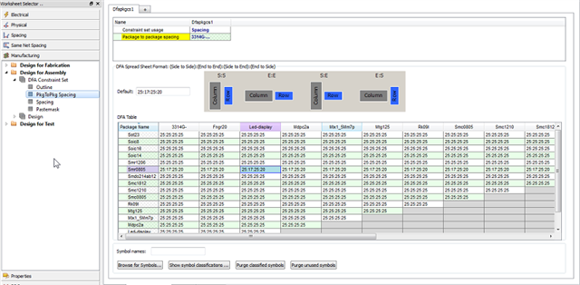
Physical spacing constraints from the spacing and same-net spacing categories, drive the clearance between the shape and nearby objects. These will include via, pin, drill hole, mechanical hole, cline, text, and shape to shape spacing. But, with the hierarchical, advanced constraint structure available with Allegro® Constraint Manager, this is taken to a new level. The spacing will differ depending on the nets of the conflict item and where it is on the board relative to constraint regions.

The base spacing constraints are augmented by the shape parameters. Available at the shape instance level or the global design level, these allow you to add any additional spacing needed between the shape and that object type. All locations in the database must always snap to the defined manufacturing units and accuracy. Depending on the accuracy of your design relative to object sizes, this oversize allows you to control how the tool compensates when it cannot meet the spacing rules exactly. You can also control the pad types used (do you need to void to the regular pad for vias, or maybe you need to void to the anti-pad) and the thermal connections needed. If a full contact is required for a pin, then the pin’s origin point must overlap with the shape.

Shape rules in Constraint Manager

Lastly, in rare cases, you may need additional clearance on a specific object. Maybe you have a set of critical traces you want extra spacing around. Or this via shouldn’t be voided at all. Properties on those individual clines allow you to accomplish this exact tweak while maintaining it as you continue your design work.

Effectively Managing Your Dynamic Shapes and Voiding

With the number of rules to satisfy, it is reasonable to fear that having the system monitoring and managing this constantly while you work could lead to slow, inefficient design. Not so! Proper use of the tool will keep you moving fast without sacrificing design intent or feedback needed to make intelligent choices.

Place your components before you add your dynamic shapes. There is no need for the shapes to be there before there is anything to void to. Once you have your components laid out and are happy with the net scheduling, add your shapes. This should be done initially in rough or fast mode. While you are planning and placing initial routing, it is important to see if your shape integrity will be affected. But, it is far from the time when you need the shapes to be ready for artwork. After all, you can’t generate artwork when your components aren’t even connected! With initial routing complete, transition to smooth mode for your shapes. This will allow you to see the exact, detailed impact of your changes to the overall layout and metal density. If you have concerns about the metal coverage in areas of your design, Allegro offers tools to help monitor and guide you in this area, as well.

Avoid running the tool in smooth mode when you are making large changes to the entire design unless you are sure it is necessary. The time the tool spends trying to keep your shapes up to date during a batch update is likely to be far longer than just forcing them to update after all the complete batch of changes has been made.

Benefits of Updating to the Latest Release

With every release, whether it is major, minor, or quarterly update, improvements are made to fix bugs, add new functionality and improve the performance of both static and dynamic shapes. As a core technology in the PCB and IC package layout, these are always high on the list of focus areas.

In the recent 17.2 quarterly update, improvements to voiding accuracy around clines should be immediately noticeable. As your cline moves through constraint regions, not only does the trace neck up and down, but so does the shape to trace clearance. Clearance around the trace remains consistent across the entire path, as well, for SI reasons. If you need to add instance-level parameter overrides (or clear them) on multiple shapes, do so with the shape edit application mode. This will let you select them all together and make the changes, rather than applying changes one shape at a time.

3D Canvas

Expect a similar level of new capabilities and enhancements, targeted to get your design to market as easy and as rapidly as possible, in the future.

BoardSurfers: Validating Your Shapes

$
0
0

BoardSurfers: Cadence Allegro BlogYour design is near completion. Except that you’ve got an area of your plane shape that stubbornly refuses to fill, and you don’t know why. Understanding the rules involved and the tools available to help you figure out – and make changes, if needed, to get the result you want – is critical to make sure you aren’t wasting valuable design cycles.

Thankfully, the Cadence® Allegro® platform provides you with the exact checks that you need from start to finish. This post will cover those available tools plus when, and why, to apply them to your design.

Corrupt Shapes

While rare, it still happens at times that a shape outline in your design will become corrupt. It can be difficult to recognize this when it happens, but triggers that can visually show this are incorrect display of the shape (an area that should be voided appearing solid) or incorrect DRCs (reporting a violation that visually looks correctly spaced). To check for this, run DBDoctor from the Tools menu with the check shapes option enabled. If any shapes have problems, which could range from duplicate void elements to self-intersecting outlines, they will be reported in the results along with the net, layer, and reference location. If DBDoctor cannot decisively determine the intended shape, you will need to edit it yourself. Often, it is as simple as deleting and recreating the dynamic shape boundary, which is usually a simple outline.

Unfilled Shapes

If a shape doesn’t fill where you believe it should, there are a selection of potential causes. The number one cause is typically that the shape would be too narrow in that area. Areas narrower than your minimum aperture width cannot be filled. Consider spacing surrounding elements farther apart (we will assume you can’t just change your manufacturing capabilities!). A similar cause may be that the shape’s area is under the minimum shape area specified in the global shape parameters or, if you have enabled automatic island and antenna deletion, the shape may have been suppressed due to insufficient connections.

Shape with islands deleted

Wrong Net Shape Filling an Area

Rather than having an area with no fill, sometimes you will have cases where the fill in an area is associated with the wrong net. In this case, what to look for is very specific. In the Allegro layout tools, all dynamic shapes have an assigned priority. Higher priority shapes fill an area first, with lower shapes pouring only in the empty space remaining. Should you find an area with the wrong shape fill, check the fill priority for both shapes and adjust them to correct the pour ordering. In some cases, if you nest shapes inside of other shapes, it may be necessary to cut the shape into multiple pieces to get the priority you need in specific regions.

And remember: static shapes always have the highest priority! They cannot void automatically to surrounding shapes as dynamic shapes do. So, they will always fill where they are placed.

Spacing to Surrounding Items is Too Great

See our earlier blog entry about how dynamic shape voiding works. Of all the potential issues, this can be the most difficult to analyze. A first step is to use the show constraint tool to confirm the spacing required between the shape and the other element at the location provided. If you have a constraint region with larger spacing, or a net-net constraint, the voiding may be a result of these values. If that proves correct, then look at the object to see if there are properties specifying additional spacing needed from the shape. Lastly, it is possible that another object nearby, also in need of a void, has caused the shape to pull back here (indirectly, due to artwork requirements like minimum aperture).

Validating Before Going to Manufacturing

Having fixed all known issues with your shapes outlined above, you are ready to go to manufacturing. Before you can do so, there are a few steps that you must run. Some are required before output, like Gerber may be generated, others are good practices.

Make sure that your shapes are all up to date in smooth mode. You cannot generate artwork or other manufacturing outputs if shapes are not all up to date in smooth mode, since the artwork would not respect all the design rule requirements. You can check the shape status from either the global shape parameters page or from the status dialog and use the Update to Smooth button in either if needed.

Enable and run the DFM design rule checks for shapes. These provide you with solid, dependable checks for everything from acute angle corners to minimum widths across the entire design. Don’t rely on downstream tools to give you errors. Find them and fix them before you ever generate artwork!

Design for Assembly DFA rules in Constraint Manager

Run the shape check tool on shapes. This function will run a comprehensive check on the shape based on a specified aperture value. It will flag (circle figures in the canvas) areas that cannot be manufactured for any reason. Depending on where the issue is, you may choose to use a route keepout, add extra clearance to the object in the void, or edit the boundary of the shape directly. You can run the shape check tool again when you’ve made changes to confirm that there are no lingering problem areas.

Generate a shape report. Available from the Tools menu, the report will include all the shapes in your design, along with their artwork settings, cross-hatch parameters, and other details, such as area of fill relative to area of the boundary shape.

Benefits of Updating to the Latest Release

With every release, Allegro strives to improve its shapes tools and quality of results. From bug fixes to performance enhancements and new functionality as requested by you, the design community, you will always find helpful updates with every major or minor release.

In 2018, a new shape voiding engine was released. It eliminated almost all instances of shape spike and unfilled region problems while improving performance. This alone would be a great reason for anyone to update their software and take advantage of. When combined with a host of new voiding options and bug fixes, the option becomes ever clearer.

Viewing all 674 articles
Browse latest View live