Quantcast
Channel: Cadence PCB Design Blogs
Viewing all 666 articles
Browse latest View live

Why Move Up to Allegro 17.2-2016? Via Structures - The Next Generation High Speed Routing Solution (Reason 8 of 10)

$
0
0

Via transitions are very common for signals. And in high speed frequencies, these via transitions can be a major contributor to signal degradation in PCB interconnects. High speed channels require ground via(s) close to critical signals to reduce loss of signal integrity by providing continuous return current path when signals transition layers.

If you are a PCB design engineer, you know very well that layout implementation to meet these requirements can be complex and time consuming. Oftentimes, current methodologies employed are manual, tedious, and prone to layout errors or misses. It is easy to forget to add return path via(s) on critical signals, or leave behind the return path vias when the critical signal routing has been moved. In addition, adding custom voids around high speed diff pairs when they transition between layers is a cumbersome manual process today. And the nightmare doesn’t end there… how about if you need to make edits to the hundreds of high speed via transitions with return paths you painstakingly placed in your design because they don’t meet specs? Talk about hours if not days of re-work.

This is why we came up with the new High Speed Via Structures – a unique methodology that allows you to create reusable elements where you can define correct-by-design high speed via transitions with custom return paths and voids.


Now, it is a whole lot easier and faster to place any repeated routing patterns in design or re-use them in other databases – think complex high speed structures, custom diff pair gathers, various test structures, and breakout patterns … the possibilities are endless of what you can define as Via Structures. 


The Via Structures also stay together during placement and interactive editing so they can never be unintentionally altered, a very important feature to ensure the design intent always remains intact.


But what really sets Via Structures apart is its ability to easily handle changes. Made a mistake? No problem, modifying and replacing any or all of the placed Via Structures with a different Via Structure is a breeze.


Want to quickly replace a thru via with stacked blind buried vias and also add a return path via? Breathe easy. We have a Replace Via with Via Structure option as well.


Via Structures provide a faster and easier mechanism to meet today's complex high speed signal routing requirements. Explore and harness the power of Via Structures today!


Related Links

Back to “10 Top Reasons to Move Up to Allegro 17.2-2016 Release

Related material on "What’s New in Allegro" on Cadence.com


Learning Advanced Flex and Rigid-Flex Design Support in Allegro 17.2-2016

$
0
0

Allegro PCB Editor now offers Rigid-Flex applications where it’s common to have different fabrics across the final PCB product. The new functionality offers integrating more technology into less material space. This technology enables design flexibility way beyond conventional rigid interconnect methods. Rigid-flex consists of flex circuit(s) that are laminated within a rigid dielectric material. Base Material for flex is generally Polyester or Polyimide. The most common metal is Copper that is Rolled and Annealed (RA) as it is less prone to cracking under stress. Electrodeposited (ED) can be used for thinner foils. Coverlay is the material laminated to the outer layers of the flex circuit to insulate the copper conductors. Soldermask does not bend as well as polyimide or polyester.

Single Sided Flex Construction of Rigid-Flex

How does Allegro PCB Editor help me with Rigid-Flex design?

The Cadence® Allegro® and OrCAD® 17.2-2016 release enables several new capabilities that minimize design iterations and lower overall cost for flex and rigid-flex designs.

Cross Section Support of Non-Conductor Layers

The Cross Section Editor now supports the entry of non-conductor layers; typically mask & coating layers used in rigid, flex or rigid-flex applications. These layers are usually added above the Top or below the Bottom surfaces but can also be added within the core stackup to accommodate multiple independent flex laminates.

 The new Surface Finishes Class supports the following subclasses …


Multi-Cross Section Support

The Cross Section Editor has been enhanced to support multiple stackups, each capable of supporting conductor and non-conductor layers such as Soldermask and Coverlay. The Cross Section Editor provides total thicknesses for each stackup in terms of accumulated conductor layers as well as a mask layer option.

Physical Zones

Zones represent physical areas of the board that differ in layers/materials - rigid flex, material inlay.

 The Zone Manager displays each zone placed in the design. It allows an easy way to assign physical zones to the stackup. You can view the Start/Stop layer of the Zone. Assign any existing Constraint Region to the Zone.


Inter Layer Design Rule Checks

Provides the ability to check geometries on two different Class/Subclasses used in rigid-flex designs. In typical Rigid Flex designs the creation of various masks, bend areas, stiffeners, etc. require special clearances or overlaps of materials and spacing. These objects are represented on specific subclasses that require a verification process to ensure that the clearances and overlaps are properly met. The Inter-Layer Checks provide much of that capability.

We will be posting more on the new functionalities in Allegro 17.2. Use the "Subscriptions" box at the top of this page to subscribe to this "PCB Design" blog to get updates.

Related Links

Why Move Up to Allegro 17.2-2016? Advanced Flex and Rigid-Flex Design Support (Reason 1 of 10)

Cadence Allegro Rigid-Flex Overview on Cadence.com

Ensuring Reliable Products with New Rigid-Flex Design Rules

Why Move Up to Allegro 17.2-2016? New Design Level Checks! (Reason 9 of 10)

$
0
0


The Allegro PCB 17.2-2016 release is loaded with enhancements related to the DRILL.

We have added Pad Definition support for the Actual Drill Tool, Backdrill Tool, Square Drill, Counter Bore/Sink objects and expanded tolerance for slots. By popular demand, Backdrill sites are now fully supported with DRC clearance rules (Top 10 Reason #4).
Also new is a behavioral change to the standard Drill Hole Spacing DRC. Back in release 16.2, we provided the Drill Hole DRC to support the “Dynamic Unused Pad Suppression” application. The check only functions when the pad is removed or is smaller than the drill hole size (spotter pad). Since that time there has been heavy demand to support the Drill Hole check, whether the pad is present or not.

Enhanced Drill Hole DRC

In Allegro PCB 17.2, a new Spacing Options toggle control has been added to the Analysis Modes – Design Mode menu called ‘Check holes within pads.’
• When the toggle is ON, drill-hole checks are run using the drill hole explicitly (the presence of pads associated with the drill hole is not relevant in this mode of the DRC calculation). In other words, the drill is checked whether a pad is present or not.
• When the toggle is OFF, the drill-hole checks are only relevant when the pad is suppressed or undefined exposing the bare hole. This is the default configuration and is compatible with previous releases.


Acute Angle Detection 

A suite of four angle based checks are introduced as Design Level DRCs. The acute angle checks are enabled through the new Setup-> Constraints -> Modes command, then selecting the Design Modes (Acute Angle Detection) entry in the Analysis Modes form. The DRC mode may be set to On-line, Off, or Batch modes while the angle values can be set in the range of <0: 90> degrees.


When an Acute Angle DRC is viewed, the DRC marker contains the Characters “AA” to identify the DRC as an Acute Angle violation. The Acute Angle DRC Checks performed are:

Minimum Shape Edge to Edge Angle
The copper shape outline has an acute angle of less the angle specified. 


Minimum Line to Pad Angle
Cline to pad entry has created an acute angle of less than 90 degrees.


Minimum Line to Shape Angle
The cline to copper shape intersection has created an acute angle of less than 90 degrees.


Minimum Line to Line Angle
The cline to cline intersection has created an acute angle of less than 90 degrees.


Net Class-Class Rule Assignments

Many of you have voiced your concerns to us about the way we display Net Class-Class rules in Constraint Manager. The feedback submitted to us was the current implementation is redundant and difficult to comprehend. I am happy to report our Constraint Manager team has provided an option to view the rule assignments in a two dimensional array. Navigate to the Spacing Domain – Net Class-Class worksheet where the new “Cset assignment matrix” is located.

Related Links

Back to “10 Top Reasons to Move Up to Allegro 17.2-2016 Release

Related material on "What’s New in Allegro" on Cadence.com

What’s Good About Allegro PCB Editor New Concurrent Team Design? New Capabilities in 17.2!

$
0
0

The 17.2 Allegro PCB Editor has new concurrent team design capabilities.

For details, please read Michael Catrambone’s blog - Why Move Up to Allegro 17.2-2016? New Concurrent Team Design Capability (Reason 2 of 10).

Concurrent team design (PCB team design) has been part of Allegro PCB Editor for some time now; the capability requires the partitioning of the master design into separate sections so each of the team members can perform their design activities. These sections are exported from the master database as partition databases, so each team member can work independently on their assigned section. Once work is completed, the individual design partitions are imported into the master database so that all of the team members' work can be reviewed in one database and any possible conflicts that may arise can be resolved. This has been a productive way of allowing multiple users to work on one design; however, because each team member is working on a separate partition, you really cannot get a clear picture of the design through the design process without disrupting design activities with an import process.

In 17.2, a new concurrent design solution allows you to connect to a common database to perform collaborative design activities. Each team member can see the design updates in real time. These design updates are being updated to the common database, so there is no need to generate or import design partitions to see other team members' design work.


Read on for more details…

At a high level, concurrent team design works in the following manner:

  • Allegro clients connect to the server application which has the master database open
  • Each client will pull the database from the server into the Allegro environment to work on the design and dispatch changes they make back to the server
  • The server will then integrate the changes in the master database and dispatch to other clients


The user interface includes:

  • Current open database and user (owner) that started the server
  • Three convenient buttons to Open, Close, and Save the database
  • Three additional tabs to monitor who is connected to the database, which objects are locked by team members, and a general log of server activities

GUI

There are several server options available where you can control the following:

  • Maximum number of clients that can connect to the database at any given time (the default is 5)
  • The TCP-port range available for server-to-client communication
  • Enable auto-save
  • Security tab
    • Access control list: allow or deny access lists based on user name
    • Passkey: set custom or auto generate a password that will be required when client connects to the server database

Options

Security1    Security2


Using the Allegro PCB Symphony Team Design option you will see two additional entries under the File Menu - Symphony Connect… and Symphony Start Server…

File > Symphony Start Server…
This will open the Symphony Server application and share the currently saved database so it can be available for multiple clients to connect to the same database and perform design activities in a concurrent environment.

File > Symphony Connect…
Once an Allegro database is opened by the Symphony Server it will be visible under a particular TCP port on the host machine (server) available for clients to connect to the database.


You can read the highlights of the 10 Top Reasons to Move Up to Allegro 17.2-2016 Release.

Please watch our Webinar on Allegro PCB Symphony Team Design.

You can review more details at the 17.2 Launch Page


As always, I look forward to your feedback!

Jerry “GenPart” Grzenia

OnDemand links to our Allegro PCB & PSpice 2016 Webinars and looking to 2017...

$
0
0

As we wrap up 2016, I wanted to share the quick access links to all of our OnDemand Webinars from Q4 2016.

** Also, we are collecting your wishlists for 2017 webinars here. **

Please click this link to participate in our 2017 webinar survey.

Boost Your Circuit Simulation Performance with New PSpice Engine

Learn how to accelerate your designs with the improvements in Cadence PCB 17.2-2016. Watch this webinar to see how the latest advancements in PCB design technology can help you to reduce back-and-forth with the mechanical team by getting your rigid-flex design right the first time, save time routing arcs with contour hug trace to quickly add arc routes, and. create better backdrills automatically

https://www.cadence.com/multimedia-secured.html/content/dam/cadence-www/global/en_US/videos/tools/pcb_design_analysis/PCBSecured/boost-circuit-simulation-with-pspice-webinar.mp4  

Accelerate Your PCB Designs - Stay Current with Improvements in Allegro PCB 17.2-2016 Release

PCB design is a never-ending cycle—the sooner you can finish one design, the sooner you can get started on the next. Join our webinar and learn how the latest advancements in Cadence® PCB 17.2-2016 technology

https://www.cadence.com/multimedia-secured.html/content/dam/cadence-www/global/en_US/videos/tools/pcb_design_analysis/PCBSecured/accelerate-pcb-designs-webinar.mp4

Gain an Unfair Advantage - Make Better Products Faster with Cadence PCB Tools

They’re coming for you, and they’re coming with everything they’ve got. Your competition has set their sights on your company, your product, you. What can you do, as the PCB designer, to make better products, faster? • Complete your designs faster: Automate manual tasks and calculations like differential-pair tuning, timing, and use interactive routing. • See the forest through the trees: Find new ways to solve design problems by planning routes so you can make the impossible, possible. • Get it right with manufacturing the first time, every time: Cut design-related manufacturing issues with real-time in-design manufacturing rule checks and the latest IPC-2581 standard. In this live webinar, learn how your Cadence® PCB tools can help you crush your competition.

https://www.cadence.com/multimedia-secured.html/content/dam/cadence-www/global/en_US/videos/tools/pcb_design_analysis/PCBSecured/allegro-pcb-gain-unfair-advantage-webinar.mp4  

Serious Tools for Rigid-Flex - Avoid Costly Fabrication Errors with Real-Time Inter-Layer Checks

Rigid-flex technology lets us create smaller PCBs than ever before. And these PCBs are making our lives better in the form of wearable, mobile, and medical devices. That’s exactly why failure is not an option. The stakes are high when devices are so personal. Real-time inter-layer checks prevent errors with coverlay and mask to pad, precious metal to coverlay, and bend area/line to stiffener, component, pin, and via. And complete those cumbersome last routes with arc-aware routing modes. Bending and folding aren't about looks; they are fundamental to the functionality of your board. Join this webinar to learn how to verify the functionality of your rigid-flex designs.

https://www.cadence.com/multimedia-secured.html/content/dam/cadence-www/global/en_US/videos/tools/pcb_design_analysis/PCBSecured/rigid-flex-inter-layer-checks.mp4  

Team Source Your PCB Layout - Hassle Free Real-Time Team Design

Show, share, and collaborate on your most complex PCB designs in real-time, without setting up a dedicated server. Allegro® PCB Symphony Team Design Option is the easiest way to collaborate on your designs.

https://www.cadence.com/multimedia-secured.html/content/dam/cadence-www/global/en_US/videos/tools/pcb_design_analysis/PCBSecured/team-source-allegro-pcb-symphony1.mp4


Related Links

Back to “10 Top Reasons to Move Up to Allegro 17.2-2016 Release

Related material on "What’s New in Allegro" on Cadence.com

Why Move Up to Allegro 17.2-2016? Vince’s Favorite Usability Features! (Reason 10 of 10)

$
0
0

Most of the PCB designers I know are creatures of habit just like I was...

we have our favorite colors, layer names, customized keyboard and our number one goal is to see how many nets we can route in one day. Very rarely do we change – but when we do it’s either because we changed employers or we are forced to because the tried and true processes don’t work any longer.

Can you relate?

Those of you who were fortunate enough to attend past CDN Live conferences may remember that, as a customer I used to present a session called “Allegro Tips – Did you know … ? In all fairness, my presentations were called that because I was an Allegro user, but having joined Cadence roughly two years ago I have come to hear from and appreciate the many loyal OrCAD users out in the community that are creating some bleeding edge designs.

So, back in early 2016, at the last CDN Live Silicon Valley edition, we revived this very informative session – at least that is what some of you told us – but this time with a new name – “Cadence PCB Editor – Tips & Tricks – Did you know … ?” As a secondary piece to this revival, we are also starting a similar blog that hopefully will give all users of Cadence PCB Editors valuable tips and tricks that may make you stop and think about different options open to making your design process faster and easier and hopefully more productive. Change can sometimes be good for you.

Therefore, without further ado, with my opening blog, I offer up to you, our valued readers, Vince’s Favorite Usability Features from V17.2-2016. We hope you find them very informative and helpful. Check back soon for additional PCB-related blogs.

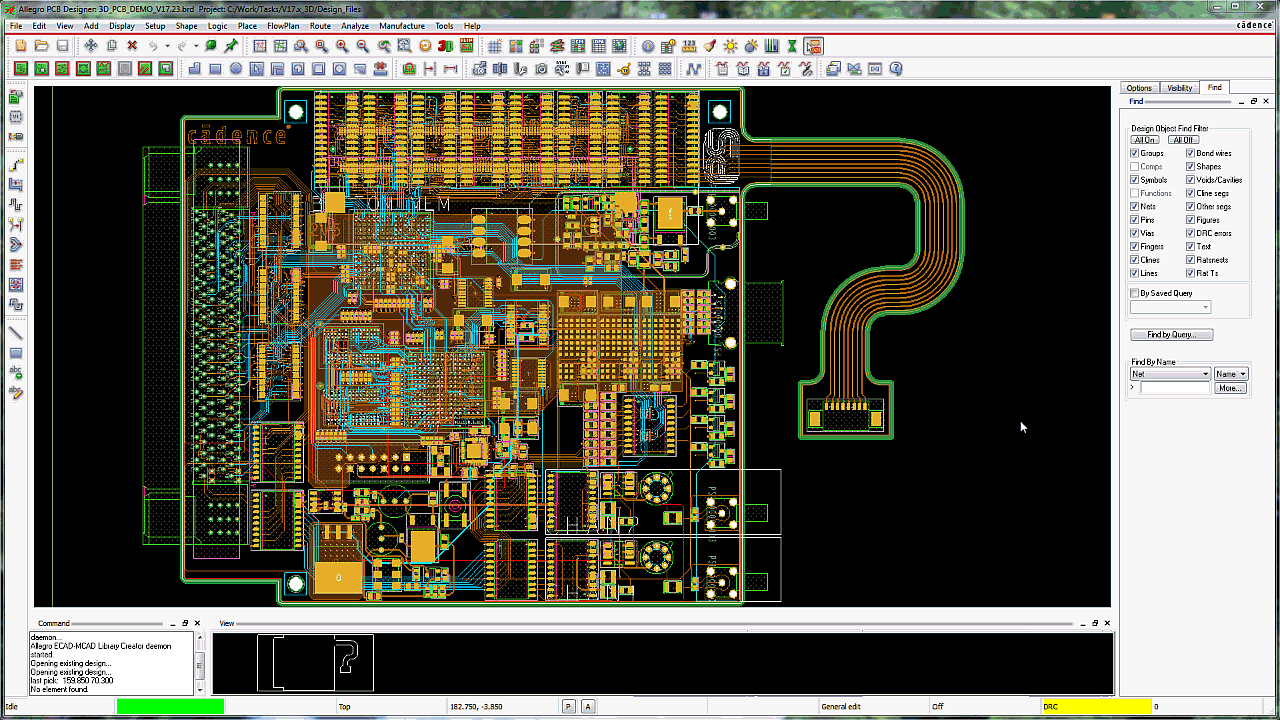
1: FbQ – Find by Query

We introduced a new and powerful relational query engine in the V17.2 QIR1 release. You can use FbQ to easily and quickly locate design objects within any size of design – large or small. With a few simple clicks, users can create, use, save and recall time saving queries.

Have you discovered how powerful this new feature can be?


2: Customizable Visibility Pane

We enhanced the Visibility Pane to allow designers more efficient access and control of layer content. Instead of a single stackup approach, the Visibility Pane now gives you quick access to different Zone stackups if you are designing rigid-flex PCBs. This pane now has the added benefit of being able to control layers other than electrical.

Customization of the Visibility Pane is done from the Visibility Pane tab in the Color Dialog.

Using the Visibility Pane Configuration settings, a user can tailor the Visibility Pane to their liking by turning on/off the following information rows:

  • Global Visibility
  • View Selection
  • Layer Stackups Selection*
  • Layer Conductors
  • Layer Planes
  • Layer Masks

*Note: Stackup Selection with the Layer Stackups dropdown will only be available (for turning on or off) in designs that contain more than one zone in the stackup.


You can also configure which columns to display in the Visibility pane. Simply drag and drop or use UP arrow to add classes to the Visible Classes sections so that they are visible on the Visibility Pane.

"Board Geometry” added in the above step is now added to the Visibility Pane.


Use the sliders to control the size of the color boxes as well as the spacing between the color boxes on the Visibility Pane.

Slider to control color boxes:  

Smallest button size with largest spacing:                                                 

Largest button size with smallest spacing: 

Color control made easy. Let us show you how!!!

3: Layer Select Mode

We enhanced the Visibility Pane to allow the user to go into “Layer Select Mode”. This action puts the canvas into a “single layer” view and allows the designer to quickly view or scroll through each of the layers available in the Visibility Pane. When Layer Select Mode is enabled, the layer names change to blue HTML links.


HTML links allow users to switch from one individual layer view to any other. Simply click on any of the Layer Names and the canvas will change to that particular layer.

When in Layer Select Mode, any combination of multiple layers to be selected and viewed using CTRL+Layer to select.

Trying to find routing channels for those last few hard to get in connections?

Use the power of Layer Select Mode to help you!!


4: FbQ & Multiple Copper Shapes

We improved dynamic shape parameters to enable users to select multiple shapes and view, edit or assign parameters, which will then apply the changed settings to each shape. Users also have the option to reset all parameters to the Global Default settings with a single click. Using SHIFT or CTRL + Click to select multiple shapes, performing a RMB in QIR 1 gives users an enhanced "Parameters” selection (as shown on the right screen shot – the left screen shot is pre-QIR 1.

The Parameters dialog for multiple selected shapes has been enhanced to indicate the information that is different between the selected shapes and what settings have been changed from the Global Shape Parameters settings.


But the real hidden power of this new feature is to combine it with the power of FbQ– which we discussed earlier in this blog. Simply use FbQ to isolate the required copper planes, select those planes from within the Matching Objects pane and then use the RMB to access the Parameters dialog. Make the necessary changes and apply them to all of the selected copper shapes at once.

How easy is that! 

5: FbQ & 3D Canvas

Another feature that the power of FbQ can be harnessed to promote is the new 3D Canvas. This new 3D Canvas has taken our previous 3D Viewer and added intelligence. Additionally, unlike some other tools that make designers function either ONLY in the 2D space or the 3D space – but not both at the same time – we have re-written the 3D Canvas so that it can be visible, functioning and even more surprising to some – communicating with the 2D canvas.

If you find this intriguing, stay tuned for a future dedicated blog on our new 3D Canvas. In the meantime, allow me to once again demonstrate how two very different features of Cadence editors can be brought together to make the power of two even more productive for designers.

Using FbQ designers can easily select any critical routed traces and then invoke the 3D Canvas to review those routed traces in 3D. See them traverse layers and see them with their attached pads and pin padstacks. How cool and beneficial is that? You can do the same thing with components – either from within the PCB Editor canvas or from within the Symbol Editor tool. Now users can take advantage of the 3D canvas to visually confirm that their components are created correctly.

We hope you have found this blog helpful. Please check back periodically as new and related blogs will be added by our very experienced and resourceful team.

Thanks again and we look forward to your next visit.

Happy designing !!

Related Links

Back to “10 Top Reasons to Move Up to Allegro 17.2-2016 Release

Related material on "What’s New in Allegro" on Cadence.com

See our YouTube Cadence Allegro Channel and the following "ease of use" video.

(Please visit the site to view this video)

PSpice – A SPICE Tool Way Beyond Functional Simulation Being Showcased at CDNLive Silicon Valley on April 11, 2017

$
0
0

 Every year Cadence Design Systems an industry leader in the Electronic Design Automation Industry hosts worldwide CDNLive forums where Cadence technology users and technical industry experts showcase their latest innovations using Cadence technologies associated with designing Digital ICs, Mixed-Signal ICs and PCBs.

This year at CDNLive Silicon Valley from April 11th to April 12th the PCB simulation session track is showcasing PSpice simulation-focused presentations by Texas Instruments, Spero Devices, MathWorks and Cadence. Topics for this year include

  • Improving design manufacturing yield and reliability
  • Process improvements on PSpice model integration within the Spectre Circuit Simulator
  • Customization of the web-based Texas Instrument power supply design simulator with Allegro PSpice Simulator
  • Algorithm to Implementation: Combining MATLAB and Simulink with PSpice to streamline PCB design
  • Innovative Memristor technology leveraged with PSpice CMOS Analog Co-Processor for Acceleration of Performance Computing Applications

Click here to register.

For more innovative technologies being leveraged with PSpice, check out http://www.pspice.com/

Jerry "GenPart" Grzenia

Epic Western Movies and PCB Design. Seriously.

$
0
0

I love that recently Westerns movies are making a comeback. Something about the romanticism of a hired gun coming in with no baggage, looking at the situation pragmatically, and doing what everyone knows needs to be done, but just can’t.

Once Upon a Time in the West and The Good, the Bad and the Ugly, Sergio Leone’s epic Spaghetti Westerns, aren’t the only foreign influence on what we think of as American Westerns.

Some might say that the greatest Western ever was Japanese director Akira Kurosawa’s Seven Samurai. The plot is simple: a small village harassed by criminal bandits, hires seven warriors to fight them off. Sound familiar?

The hired warrior isn’t afraid to kill a few bad guys. And then they leave and peace is restored. Japan has long had the concept of a hired gun. The characters 助っ人 (suketto) in Japanese are ‘helper person’ and are used to describe many situations, even PCB design.

They do what the regular team can’t—or won’t—do, but everyone knows needs to be done. I like to think that sometimes our PCB design teams work the same way.

Designs are getting so complicated that it’s rare to find someone who knows everything about everything and can do it all alone. So we have our in-house suketto or hired guns.

These experts that can come in, quickly assess the problem, do what needs to be done and get out so that the rest of us can get back to our regular lives.

But there’s a problem. PCB design isn’t shooting a couple of bad guys. Everyone else doesn't hide in the church, we all need to keep on designing.

That means we can’t divvy up a design into segments because the lines of your domain and mine are not geographical, they’re technical. My buddy is the expert in DDR4 high-speed routing, but I still have to do my work while he’s helping me out.

This situation is pretty common with lots of our customers. They have teams around the globe and many domain experts scattered throughout the teams. They came to us for a way to leverage these talents without disrupting design projects, locking down files, or involving IT.

Now, our customers have a distinct advantage over their competition. They have hired guns taking out the bad guys for them all while shortening their design time.

How much shorter?

Check out this handy calculator we put together and find out how much time you could be saving.


Why Move Up to Allegro 17.2-2016? So How Does Your Design “Stack-Up”? (Reason 5 of 10)

$
0
0

We are not talking about how your design compares to the next guys’, we’re talking about the PCB layer structure of your design, be it rigid, flex, rigid-flex, or using inlay technology. Stackup definition, more specifically accurate stackup definition, is critical for a wide variety of reasons. The arrangement of the various materials affect the computations and analysis for controlled impedance nets and cross talk reduction which drives functional performance. ECAD/MCAD collaboration that expresses true substrate thickness, including mask layers is critical in modeling the physical aspects of a system, especially for those smallest or thinnest of devices that require the most efficient use of space. Most importantly, an accurate stackup definition is sent to the board fabrication facility for producing a final product that performs as the design data intended.

Material Inlay 


Rigid-Flex


Cadence® Allegro® PCB Designer 17.2-2016 makes it simple to define an accurate stackup structure for each of the design types previously mentioned. Our new Allegro PCB Editor Cross Section Editor provides the ability to define the dielectric and conductor layers, as well as external mask layers for rigid and flex designs. The Cross Section Editor enables you to easily define stackups for those single designs that must incorporate different stackups which use a variety of both conductor and non-conductor layers for flex, rigid-flex and/or inlay structures. Assignment of material is augmented through the use of a mask site definition file connected to the Cross Section Editor. The Mask Site file is managed by the user who creates a library of materials and standard mask layer names that are preferred by their company. When defining a layer in the stack, the user selects the appropriate layer name, and the layer and material are added into the stackup structure.

Mask Site File

Adding mask layers to the stackup is a simple process when building the stackup definition. When adding layers, the Mask Site File is read, and the layer names, and materials are presented to the user. When selecting the layer type, the assigned IPC-2581 Layer Function and material are highlighted for the user to see, but if one of the attributes requires a change for the particular design, simply selecting the new attribute from one of the lists updates the current assignment.

Create Layer Form

The Mask Site File is managed through the Site File Editor. This tool manages the IPC-2581 Layer Function type, Subclass name, Class and material for each stackup layer type that may be used in a design. Maintaining this data provides consistency between designs and reduces typo’s that may occur. Once created, the Mask Site File is stored into the MATERIALPATH location where all users have access to this file.

Mask Layer Site File Editor

Easily Define Multiple Stackups in Cross Section Editor

Defining multiple stackups in the Cross Section Editor begins with enabling the Multi Stackups Mode (View->Multi Stackup mode). The user then defines the entire cross section paying careful attention to the order of layers and materials used for the design. The Primary column identifies the default stackup structure for the design. Selecting the check box in the Primary column adjacent to the layer identifies the layer as part of the Primary stackup. To create another stackup, just select Add Stackup column (or Edit -> Add Stackup, or select the tab labeled “+”), enter the new stackup name in the Create Stackup form and the new stackup is added into the mix. Assign the layers for the stackup by checking the boxes and you’re done. The Cross Section Editor also updates the graphics to the right of the stackup tables for a quick visual reference. The user can export the finished cross section definition to a Cross Section Technology file making the identical structure available for other designs.

Multiple Stackup Definitions


Remember that remark about accurate documentation? Once the stackup structure is defined in the Cross Section Editor, one of the benefits is the ability to create a stackup table for documentation. The same data defined in the Editor can be extracted to a table in the fabrication drawing which the fabricator uses in their process. The fabricator now has the information on materials and structure to build your design accurately.

Stackup Table Example.

With the new Allegro 17.2-2016 release, the enhancements to the Cross Section Editor have provided a complete approach to defining an accurate stackup definition with mask layers, consistent layer names, and documentation details. Now you ask, “Nice, but how can I use these new features in my actual design?” Look forward to the next session “Zoning In on your Design with Allegro 17.2-2016” where more will be uncovered in using Multi Stackup capabilities.

Related Links

10 Top Reasons to Move Up to Allegro 17.2-2016 Release
What’s New in Cadence® Allegro® 17.2-2016 Release


Why Move Up to Allegro 17.2-2016? Arc-aware routing with enhanced contour hug saves time to route on flex designs (Reason 6 of 10)

$
0
0

Enhanced Contour Routing is a new prototype feature in the Cadence® Allegro® PCB Designer 17.2-2016 that provides a more efficient method to add routing during Add Connect by following an existing connect line or a route keepin. This feature has been vastly improved over the legacy Contour feature by removing a continuous dialog popup, introducing a simple canvas-based two-state click use model, and enabling Shove of existing connect lines, even with Arc corners. Transitions between the non-contoured and the contoured routing are smoothed for line or arc corners.


Enabling Enhanced Contour

Once Enhanced Contour is enabled in Route > Unsupported Prototypes > Enable Enhanced Contour, the Enhanced Contour Right Mouse Button selection becomes available during interactive routing.

Two State Click Use Model

Once Enhanced Contour is activated during Add Connect, there will be a behavioral and graphical change on the canvas. When you are within proximity of a connect line or keepin, the prospective contour template will highlight and the active connect line being routed will be prevented from shoving or going closer than the desired gap (min DRC spacing plus any Extra Gap specified).

If you click while the connect line or route keepin is highlighted, you will be locked into the contour state – route will be contouring to highlighted object. If you click again, the route will then move freely away from the contour template. You can switch modes in and out of "contour enabled" at any time.

As always your comments are welcome!

How have you used rigid-flex in your designs?  What are your top three tips to share? Please sign-in above and start contributing to the community discussion.

Related Videos

Allegro PCB Rigid Flex Demo Reel


Related Links

10 Top Reasons to Move Up to Allegro 17.2-2016 Release

Cadence Allegro Rigid-Flex Overview on Cadence.com

Are You Maximizing Your Product Design? See How a Custom ASIC Can Help

$
0
0

When you push more of your board into high-performance design fabric like an SoC, suddenly you have the scope for differentiation and innovation in an SoC that you design yourself. Custom SoCs increase differentiation, reliability, IP protection, security of supply, and performance. They also decrease board size, power, BOM, and cost. Are you ready to take the leap?

Many companies are working with custom ASICs these days. Sensor companies making their sensors smarter and OEMs integrating discrete components with a CPU for smaller PCBs and more reliable, lower cost products.

Is a Custom ASIC in Your Future? Watch this Informative Webinar to Get the Answers

ARM and Cadence recently held a live webinar on the topic of custom ASICs. Phil Burr, Senior Product Manager at ARM and Ian Dennison, Senior Group Director at Cadence gave an expert presentation on the benefits of custom chips, the routes to creating your own chip, and the tools and services available to make custom chip development easier with lower risk and cost.

If you are a start-up, an IoT developer, a sensor or mixed signal company, or an enterprise new to SoC looking to differentiate your product, watch this webinar to get an idea on how to safely and cost effectively create your own custom ASICs.

If you would like to learn more about the ARM DesignStart program or the Cadence Hosted Design Solutions, go to the Accelerating IoT System Design tab under the ARM-Based Solutions page on cadence.com.

Empowering Learning: New Learning – Cadence Allegro and OrCAD Release17.2-2016

$
0
0

Interested in an easy-to-use, collaborative, and robust design-environment that reduces design cycle? Use, Cadence® Allegro® and OrCAD® release 17.2-2016.  Here are the 10 Top Reasons to Move Up to Allegro 17.2-2016 Release This enables you to accelerate your PCB design cycle. 

Get started immediately with the new release using the central page on https://support.cadence.com. It lists important links to Allegro and OrCAD 17.2-2016 documents. Visit the “one-stop shop" page to get all you need to install and use the release.

Visit the page - https://support.cadence.com/SPB172launch

These pages list What’s New, videos, application notes, migration guide, and other online help documents. In the left pane, select Getting Started for release-level information or select a product (for example, Allegro PCB Editor) for information about it.

Allegro PCB Editor

Rigid-Flex : Rigid-Flex in Allegro® PCB Editor 17.2-2016

Enhanced Backdrill : Enhanced backdrill in Allegro® PCB Editor 17.2-2016

How to slide cline segments or vias using the "IX" and "IY" incremental commands

Allegro Design Entry HDL

PDF Publisher – Watermark Support  How to set up a watermark for PDF in Allegro® Design Entry HDL
PDF Publisher – PDF / A Generation :    How to publish ‘A’ compliant PDF (PDF/A) in Allegro® Design Entry HDL

Allegro Design Entry CIS (OrCAD Capture)

Export or convert a Capture design to ISCF

Exporting Intel Schematic Connectivity Format (ISCF) in OrCAD® Capture CIS

Generate intelligent PDFs of the schematic

How to generate intelligent PDFs of the schematic with version SPB 17.2 ?

Allegro AMS Simulator (PSpice)

Frequency Response Analysis (FRA) in PSpice -  Setting up and running Frequency Response Analysis (FRA) in PSpice

How can I run advanced analysis from my normal PSpice design? - Steps to add tolerances to run advanced analysis.


Visit the page - https://support.cadence.com/SPB172launch for more.

Contact us for any questions. Leave a comment in this blog post or use the Feedback / Like mechanism within https://support.cadence.com.

Happy New Learning!

~Jasmine

Customer Support Recommends – Rigid-Flex in Allegro PCB Editor 17.2

$
0
0

Cadence Online Support has this Rapid Adoption Kit (RAK) on Rigid-Flex in Allegro PCB Editor 17.2 that introduces a flow to define unique stackups by physical zone. The Cross Section Editor in 17.2 has been enhanced to support multiple stackup definitions including support for mask and coating layers. The primary driver for this enhancement is Rigid- Flex applications where it’s common to have different fabrics across the final PCB product. Benefits will also be realized for customers designing standard Rigid PCBs. Soldermask and Solderpaste and their thicknesses can be added above/below the surface layers. Rigid PCBs may also require inlay material zones for RF/Analog circuits.

This RAK covers …

  • Adding Non-Conductor Layers to Cross Section

  • Multiple Stackup Entry

  • IPC2581 Layer Functions

  • Adding/Editing Physical Zones in the PCB Editor

Rigid-flex technology lets us create smaller PCBs than ever before. Watch the video on Serious tools for advanced rigid-flex

Cross Section Support of Non-Conductor Layers

The PCB Editor Database represents non-conductor layers as “Mask” or “Dielectric” although they may serve different purposes like coating or plating areas. To add a mask layer above layer Top, select the Top cell in the Cross Section grid then use the RMB to access the “Add Layers” command as shown in the graphic below.

The new Surface Finishes Class supports the following subclasses …

Multi-Cross Section Support

The Cross Section Editor has been enhanced to support multiple stackups, each capable of supporting conductor and non- conductor layers such as Soldermask and Coverlay. The Cross Section Editor provides total thicknesses for each stackup in terms of accumulated conductor layers as well as a mask layer option.

Multi-Stackup Grid

Layer Functions (IPC2581)

The Cross Section Editor now supports IPC2581 defined Layer Functions. These user selected Layer functions are defined as attributes in the IPC-2581 stack-up layer definition for fabrication instructions at the manufacturing level. Customers utilizing the 2581 standard for data transfer may want to consider these options. The diagram below reveals the full set of layer function options.

Dielectric layer types support the following options …

Physical Zones

Zones are physical areas in the design that map to one of the available stackups in the cross section editor. Zones are added using the standard add shape or add rectangle commands found in the Setup – Zones menu. Mapping a stackup to a Zone may occur at the creation of the Zone, or assigned through the Zone Manager after the Zone is created. Constraint Regions and Rooms may also be assigned to Zones at creation or through the Zone Manager.

When adding a Zone, you can loosely define the boundary during the creation command as it will snap to the design outline geometry upon completing the command. In the left figure below, a zone boundary is extended beyond the actual design outline. It eventually snaps to the actual design outline when the add shape command is completed.

Inter Layer Design Rule Checks

This RAK also explores Inter Layer checks that provide a new tier of checking of mask to mask and mask to other geometry types providing the user with problem detection earlier in the design to manufacturing cycle.

             In typical rigid-flex designs, various stackup definitions are assigned into different zones where the top or bottom level might differ zone to zone. In traditional workarounds, the package symbols require special attention to padstack definitions, special “flex” symbols, and so on, or use the embedded component process to place these symbols onto the correct layer for not only artwork purposes but for documentation as well. You may refer the document on Dynamic Zone Placement in Allegro PCB Editor 17.2  here. This reviews the PCB Editor's awareness of varying top surface layers in a multi-zone rigid-flex design during placement.

Click here for the Rapid Adoption Kit and for the detailed step-by-step procedures on the Rigid-Flex functionality, as well as various other aspects that are not covered in this blog.

Note: The above link can only be accessed by Cadence customers who have valid login ID for https://support.cadence.com

Related Links

Learning Advanced Flex and Rigid-Flex Design Support in Allegro 17.2-2016

Why Move Up to Allegro 17.2-2016? Advanced Flex and Rigid-Flex Design Support (Reason 1 of 10)

Cadence Allegro Rigid-Flex Overview on Cadence.com

Ensuring Reliable Products with New Rigid-Flex Design Rules

Follow Video-Embedded Troubleshooting Articles for Easier Debugging and Empowered Learning

$
0
0

Finding a way out of situations is routine in today’s ever changing world—more so in the world of tech. Our problems range from trivial to critical. Mostly, people look for simple solutions that are easy to use. How sometimes a quick note can resolve a nagging problem! And a smart solution with a video simulating steps helps resolve issues even more quickly and satisfactorily. 

This is exactly what we are now doing at Content Support Portal.  We have articles with videos showing relevant steps.

You never miss out any step while you are trying it in your designs.

Here is how it looks like:

Visit Content Support Portal for more such video-embedded articles on major products. For example, if you want to set up differential pairs in Constraint Manager so they are spaced 20 mils from other nets,  click here.


Some more examples of enhanced features elaborated in short videos within articles:

Allegro PCB Editor

Allegro Design Entry CIS (OrCAD Capture)

Allegro AMS Simulator (PSpice)


We hope you find it useful and look forward to your feedback.

Leave a comment in this blogpost or use the Feedback / Like mechanism within Content Support Portal.

~Jasmine

CDNLive China: Interviewing with Allegro R&D VP Saugat Sen

$
0
0

 Recently, CDNLive China was held in Shanghai. What are the highlights of PCB Track? What are the latest news in the industry? What are the development strategies for Cadence PCB/Packaging? We conducted an exclusive interview with Mr. Saugat Sen, Cadence Allegro R&D Vice President

Figure 1 Mr. Saugat presented Outstanding Paper Award to Spreadtrum

Figure 2: CDNLive China

Figure 3 In PCB Track. Saugat delivered a keynote speech named Enabling System-Level Design with Allegro Technologies.

Interview with Mr Saugat

After the conference, we had the privilege of an exclusive interview with Mr. Saugat. Here are your questions answered:

1, What's the development strategy of Allegro for the future hardware design?

Allegro has been evolving to address the larger issues of system design, aligned with Cadence’s strategy of System Design Enablement. We recognize that the customers’ design challenges today are inter-disciplinary. There is a need to blend implementation and analysis, there is a need to identify manufacturing issues early in design, there is also the need to enable collaboration across mechanical and electrical domains. Our strategy is to collaborate with leading customers across the world, to innovate and leverage all our technology assets to enable solving design challenges that span Chip, Package, Board and the system of multiple boards.

2. How to shorten time to market?

One of the key vectors that we are driving Allegro on is to significantly improve customer productivity. Our concurrent team design solution - Allegro PCB Symphony Team Design solution is just one example of enabling this. We are making ECAD/MCAD co-design seamless, and blending analysis and design closely. It is our endeavor to evolve Allegro to make  transformational improvements in our customers’ ability to shorten the PCB design cycle time.

3, How to ensure the success of manufacturing in the future?

We have multiple solutions to address the needs of design for manufacturing success, including new Cadence Allegro DesignTrue DFM Technology, the industry’s first solution to perform real-time, in-design design-for-manufacturing (DFM) checks integrated with electrical, physical and spacing design rule checks (DRCs). Our experience with customers leads us to believe that we need to identify the issues as early as possible in the design process so as to reduce the end to end PCB cycle time.

4, What do you think of China PCB/Packaging market?

China is clearly establishing its thought leadership in technology across multiple domains. While companies in China has been doing leading edge work in PCB for many years, we expect a similar trend in IC Packaging as well. We are fortunate to be in a position to collaborate with our customers in China. We look forward to partner with them in evolving our technology to serve their needs and our customers worldwide.

Team Allegro


Customer Support Recommends –Team Design in DE-HDL 17.2

$
0
0

Accelerating product time to market, achieving significantly higher productivity and efficiently working in global engineering teams are the key challenges being faced by designers. Team Design Authoring (TDA) feature of Allegro Design Entry HDL addresses these challenges by providing integrated team design environment. The design can be partitioned at a sheet or block level, and each designer can be assigned one or more blocks or sheets. Any number of designers can work on different parts of the same design simultaneously without interfering with each other. The various design stages can then be combined before proceeding to layout in Allegro PCB Editor. This concurrent design approach makes Allegro Design Authoring extremely productive for large designs. Designers work on the board layout and schematic in parallel.

Cadence Online Support has this Rapid Adoption Kit (RAK) on Team Design in Allegro Design Entry HDL 17.2. The RAK covers:

  • Setting up team design environment
  • Enabling team design
  • Joining team design as member
  • Working with designs in team design environment – doing check-in and check-out

Setting up team design environment

This is the first step of team design and involves accessing the user list, granting permission to users, defining Integrator roles, updating libraries and designs and setting up project shared area.


Enabling team design

After setting up team design environment, key task is to enable team design (ETD) for a project and is done by the integrator.


When you enable a project for team design, the following happens:

  • Subdesigns are assigned to team members and can be used by designers by joining the project.
  • The selected design project is now in the shared area.


Joining team design as member

After the integrator has set up the shared area and assigned ownership rights for sub-designs, designers access the project and start work on the sub-designs they own.

Working with designs in team design environment – doing check-in and check-out

The TDO user interface offers tooltips and icons to help you perform various data management tasks that include check-in/check-out and doing modifications.


Click here for the Rapid Adoption Kit and for the detailed step-by-step procedures on the Team Design functionality, as well as various other aspects that are not covered in this blog.

Also watch the video on Enabling a DEHDL project for Team Design.

Note: The above link can only be accessed by Cadence customers who have valid login ID for https://support.cadence.com

Why Move Up to Allegro 17.2-2016? Tabbed Routing - The Next Generation High Speed Routing Solution (Reason 7 of 10)

$
0
0

Improve Route Channel Utilization with Tabbed Routing

Tabbed routing is a new method in which trapezoidal shapes called tabs are added to parallel traces to control impedance in the pin field/breakout regions, and reduce crosstalk in open field regions. It is a breakthrough routing strategy that allows for longer trace lengths and more compressed routing.

Unfortunately, this new routing technology increases layout complexity and managing these tabs later in the design process can be a nightmare.

PCB layout designers rejoice! We have heard your woes and pleas for help.

Aside from providing the means to generate the trapezoidal tabs, we have covered the entire tab "life cycle" with several unique features. 


Generate Tabs

First stop is tab creation. Select mode, enter tab size/pitch values under parameters, and select parallel cline segments to generate tabs. You can also load your saved parameters to quickly generate tabs on different areas and/or interfaces.


Analyze Tabs

Perhaps the special feature we are most excited about is the capability to Analyze Tabs. It provides an integrated and more efficient way for users to validate tab count matching and pitch. Create custom rules for pass/fail criteria and cross probe violations in canvas for fast fixing. Generate custom tab count and pitch reports to suit various data needs.


Manipulate Tabs

We offer several unique features to help handle these tabs easily. Tab in the wrong location? Easy fix with Move Tab which provides ability to move a tab along segment while maintaining centerline connectivity. It also provides dynamic DRC feedback so you can easily resolve those spacing violations. Need to quickly remove some or all of the tabs? Our Delete Tab provides a fast and easy way to delete tabs by clines, cline segments, or tab instance.

Our interactive etch editing features are also now tab aware – so tabs are intelligently copied or removed along with the segments. Tabs are no longer left floating in the design when you delete or slide segments. And it is now easier than ever to copy routes with tabs and replicate to other byte groups - copy multiple clines/segments with tabs and snap to pads or cline segments.

You won’t find a more comprehensive tool for the job.   What are you waiting for?


High Speed Routing Demo Reel

www.youtube.com/watch


Related Links

Back to “10 Top Reasons to Move Up to Allegro 17.2-2016 Release

Related material on "What’s New in Allegro" on Cadence.com

Go deep with tabbed routing with this link to whitepaper.

Why Move Up to Allegro 17.2-2016? Via Structures - The Next Generation High Speed Routing Solution (Reason 8 of 10)

$
0
0

Via transitions are very common for signals. And in high speed frequencies, these via transitions can be a major contributor to signal degradation in PCB interconnects. High speed channels require ground via(s) close to critical signals to reduce loss of signal integrity by providing continuous return current path when signals transition layers.

If you are a PCB design engineer, you know very well that layout implementation to meet these requirements can be complex and time consuming. Oftentimes, current methodologies employed are manual, tedious, and prone to layout errors or misses. It is easy to forget to add return path via(s) on critical signals, or leave behind the return path vias when the critical signal routing has been moved. In addition, adding custom voids around high speed diff pairs when they transition between layers is a cumbersome manual process today. And the nightmare doesn’t end there… how about if you need to make edits to the hundreds of high speed via transitions with return paths you painstakingly placed in your design because they don’t meet specs? Talk about hours if not days of re-work.

This is why we came up with the new High Speed Via Structures – a unique methodology that allows you to create reusable elements where you can define correct-by-design high speed via transitions with custom return paths and voids.


Now, it is a whole lot easier and faster to place any repeated routing patterns in design or re-use them in other databases – think complex high speed structures, custom diff pair gathers, various test structures, and breakout patterns … the possibilities are endless of what you can define as Via Structures. 


The Via Structures also stay together during placement and interactive editing so they can never be unintentionally altered, a very important feature to ensure the design intent always remains intact.


But what really sets Via Structures apart is its ability to easily handle changes. Made a mistake? No problem, modifying and replacing any or all of the placed Via Structures with a different Via Structure is a breeze.


Want to quickly replace a thru via with stacked blind buried vias and also add a return path via? Breathe easy. We have a Replace Via with Via Structure option as well.


Via Structures provide a faster and easier mechanism to meet today's complex high speed signal routing requirements. Explore and harness the power of Via Structures today!


Related Links

Back to “10 Top Reasons to Move Up to Allegro 17.2-2016 Release

Related material on "What’s New in Allegro" on Cadence.com

Learning Advanced Flex and Rigid-Flex Design Support in Allegro 17.2-2016

$
0
0

Allegro PCB Editor now offers Rigid-Flex applications where it’s common to have different fabrics across the final PCB product. The new functionality offers integrating more technology into less material space. This technology enables design flexibility way beyond conventional rigid interconnect methods. Rigid-flex consists of flex circuit(s) that are laminated within a rigid dielectric material. Base Material for flex is generally Polyester or Polyimide. The most common metal is Copper that is Rolled and Annealed (RA) as it is less prone to cracking under stress. Electrodeposited (ED) can be used for thinner foils. Coverlay is the material laminated to the outer layers of the flex circuit to insulate the copper conductors. Soldermask does not bend as well as polyimide or polyester.

Single Sided Flex Construction of Rigid-Flex

How does Allegro PCB Editor help me with Rigid-Flex design?

The Cadence® Allegro® and OrCAD® 17.2-2016 release enables several new capabilities that minimize design iterations and lower overall cost for flex and rigid-flex designs.

Cross Section Support of Non-Conductor Layers

The Cross Section Editor now supports the entry of non-conductor layers; typically mask & coating layers used in rigid, flex or rigid-flex applications. These layers are usually added above the Top or below the Bottom surfaces but can also be added within the core stackup to accommodate multiple independent flex laminates.

 The new Surface Finishes Class supports the following subclasses …


Multi-Cross Section Support

The Cross Section Editor has been enhanced to support multiple stackups, each capable of supporting conductor and non-conductor layers such as Soldermask and Coverlay. The Cross Section Editor provides total thicknesses for each stackup in terms of accumulated conductor layers as well as a mask layer option.

Physical Zones

Zones represent physical areas of the board that differ in layers/materials - rigid flex, material inlay.

 The Zone Manager displays each zone placed in the design. It allows an easy way to assign physical zones to the stackup. You can view the Start/Stop layer of the Zone. Assign any existing Constraint Region to the Zone.


Inter Layer Design Rule Checks

Provides the ability to check geometries on two different Class/Subclasses used in rigid-flex designs. In typical Rigid Flex designs the creation of various masks, bend areas, stiffeners, etc. require special clearances or overlaps of materials and spacing. These objects are represented on specific subclasses that require a verification process to ensure that the clearances and overlaps are properly met. The Inter-Layer Checks provide much of that capability.

We will be posting more on the new functionalities in Allegro 17.2. Use the "Subscriptions" box at the top of this page to subscribe to this "PCB Design" blog to get updates.

Related Links

Why Move Up to Allegro 17.2-2016? Advanced Flex and Rigid-Flex Design Support (Reason 1 of 10)

Cadence Allegro Rigid-Flex Overview on Cadence.com

Ensuring Reliable Products with New Rigid-Flex Design Rules

Why Move Up to Allegro 17.2-2016? New Design Level Checks! (Reason 9 of 10)

$
0
0


The Allegro PCB 17.2-2016 release is loaded with enhancements related to the DRILL.

We have added Pad Definition support for the Actual Drill Tool, Backdrill Tool, Square Drill, Counter Bore/Sink objects and expanded tolerance for slots. By popular demand, Backdrill sites are now fully supported with DRC clearance rules (Top 10 Reason #4).
Also new is a behavioral change to the standard Drill Hole Spacing DRC. Back in release 16.2, we provided the Drill Hole DRC to support the “Dynamic Unused Pad Suppression” application. The check only functions when the pad is removed or is smaller than the drill hole size (spotter pad). Since that time there has been heavy demand to support the Drill Hole check, whether the pad is present or not.

Enhanced Drill Hole DRC

In Allegro PCB 17.2, a new Spacing Options toggle control has been added to the Analysis Modes – Design Mode menu called ‘Check holes within pads.’
• When the toggle is ON, drill-hole checks are run using the drill hole explicitly (the presence of pads associated with the drill hole is not relevant in this mode of the DRC calculation). In other words, the drill is checked whether a pad is present or not.
• When the toggle is OFF, the drill-hole checks are only relevant when the pad is suppressed or undefined exposing the bare hole. This is the default configuration and is compatible with previous releases.


Acute Angle Detection 

A suite of four angle based checks are introduced as Design Level DRCs. The acute angle checks are enabled through the new Setup-> Constraints -> Modes command, then selecting the Design Modes (Acute Angle Detection) entry in the Analysis Modes form. The DRC mode may be set to On-line, Off, or Batch modes while the angle values can be set in the range of <0: 90> degrees.


When an Acute Angle DRC is viewed, the DRC marker contains the Characters “AA” to identify the DRC as an Acute Angle violation. The Acute Angle DRC Checks performed are:

Minimum Shape Edge to Edge Angle
The copper shape outline has an acute angle of less the angle specified. 


Minimum Line to Pad Angle
Cline to pad entry has created an acute angle of less than 90 degrees.


Minimum Line to Shape Angle
The cline to copper shape intersection has created an acute angle of less than 90 degrees.


Minimum Line to Line Angle
The cline to cline intersection has created an acute angle of less than 90 degrees.


Net Class-Class Rule Assignments

Many of you have voiced your concerns to us about the way we display Net Class-Class rules in Constraint Manager. The feedback submitted to us was the current implementation is redundant and difficult to comprehend. I am happy to report our Constraint Manager team has provided an option to view the rule assignments in a two dimensional array. Navigate to the Spacing Domain – Net Class-Class worksheet where the new “Cset assignment matrix” is located.

Related Links

Back to “10 Top Reasons to Move Up to Allegro 17.2-2016 Release

Related material on "What’s New in Allegro" on Cadence.com

Viewing all 666 articles
Browse latest View live